

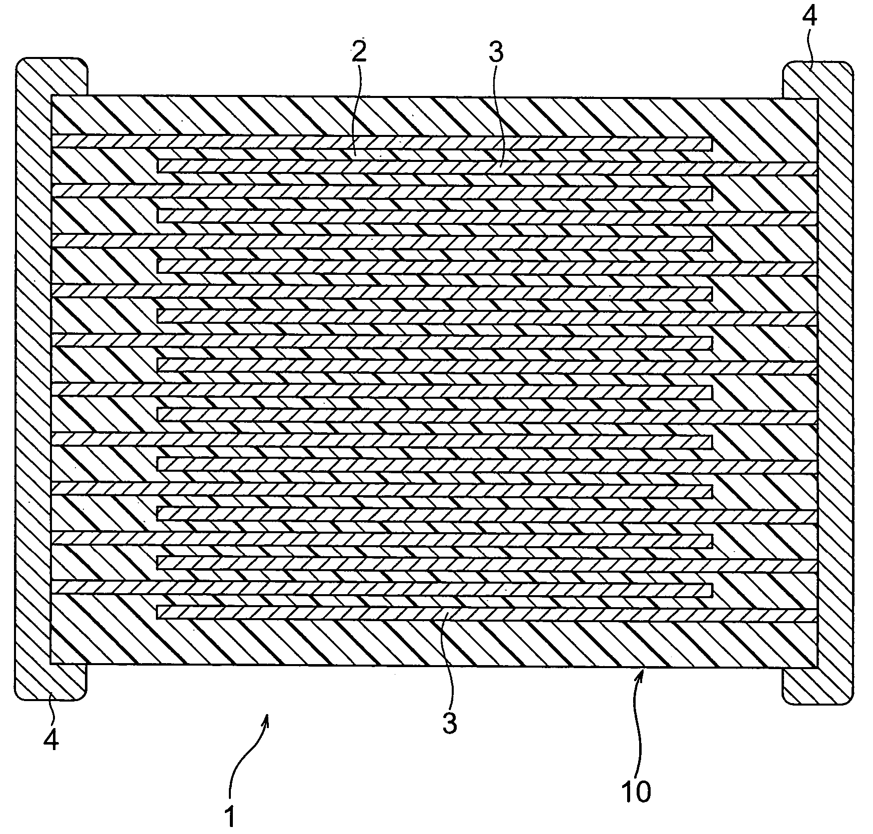
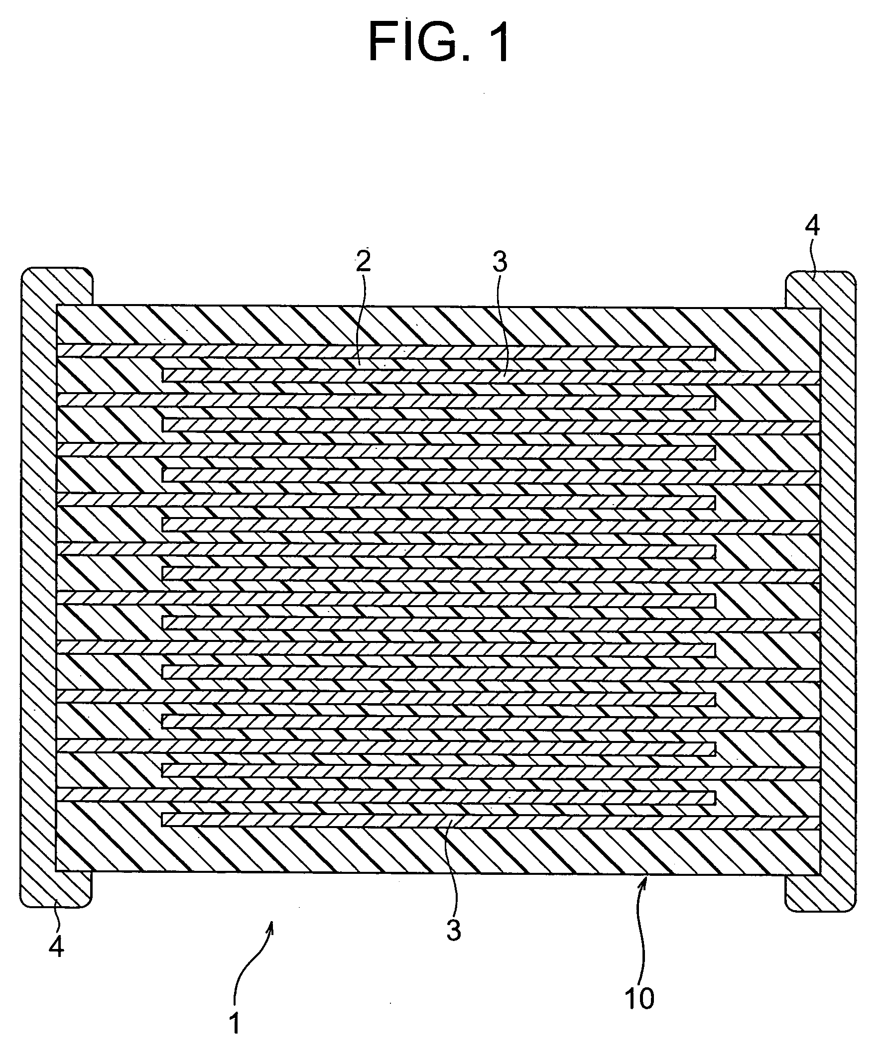
Multilayer ceramic capacitor
a multi-layer ceramic and capacitor technology, applied in the field can solve the problems of frequent cause of short-circuit defective of multi-layer ceramic capacitors, inability to use costly precious metals such as platinum and palladium, and reduce permittivity largely, so as to achieve low short-circuit defective rate, high permittivity, and preferable temperature characteristics
- Summary
- Abstract
- Description
- Claims
- Application Information
AI Technical Summary
Benefits of technology
Problems solved by technology
Method used
Image

Examples
examples
[0079] Below, the present invention will be explained further in detail based on examples, but the present invention is not limited to the examples.
[0080] As a main component, BaTiO3 materials having specific surface areas shown in Table 1 and Table 3 were prepared. Note that the specific surface area of the BaTiO3 was measured by the nitrogen absorption method (BET method). Next, the main component was added with MgO, MnO, V2O5, Y2O3, (Ba, Ca)SiO3 as subcomponents, subjected to wet mixing by a ball-mill for 16 hours and dried to obtain a dielectric material. Adding quantities of the respective subcomponents are shown in Table 1 and Table 3 by mole values with respect to 100 moles of the main components.
[0081] The obtained dielectric material was added with polyvinyl butyral and ethanol based organic solvent, mixed again with a ball-mill, and made to be a paste, so that a dielectric layer paste was obtained.
[0082] Next, 44.6 parts by weight of Ni particles, 52 parts by weight of ...
PUM
| Property | Measurement | Unit |
|---|---|---|
| thickness | aaaaa | aaaaa |
| specific surface area | aaaaa | aaaaa |
| specific surface area | aaaaa | aaaaa |
Abstract
Description
Claims
Application Information