Light emitting devices with layered III-V semiconductor structures, and modules and systems for computer, network and optical communication, using such device

a technology of layered iiiv semiconductor and light-emitting devices, which is applied in the direction of semiconductor lasers, solid-state devices, lasers, etc., can solve the problems of increasing the amount of lattice strain, difficult to achieve satisfactory high-temperature device characteristics, and semiconductor material serving as an active region

Inactive Publication Date: 2003-12-02
RICOH KK
View PDF3 Cites 34 Cited by
  • Summary
  • Abstract
  • Description
  • Claims
  • Application Information

AI Technical Summary

Benefits of technology

Accordingly, it is an object of the present disclosure to provide improved layered semiconductor structures, light emitting semiconductor devices using the layered structures, and methods of growing the layered structures, having most, if not all, of the advantages and features of similar employed structures and devices, while eliminating many of the aforementioned disadvantages.
In addition to the above-mentioned methods of improving the crystalline quality considering primarily the degree of lattice strains and critical thickness, the crystalline quality can also be improved by including a small amount of Al.
Since the present method also facilitates the layer growth to possibly be carried out under a wider range of conditions to be optimized for the layer growth, such as, for example, the growth temperature and feeding rate of source gasses, to thereby be able to attain satisfactory crystalline quality for light emissions.
With the present structure of layered III-V alloy semiconductor, a conduction band discontinuity may be formed with sufficient magnitude for preventing overflow of injected carriers. This yields the fabrication of laser diodes having improved temperature characteristics, which is useful for fabricating durable laser diodes with longer emission wavelengths.
As a result, light emissions at the wavelength region of 1.3 .mu.m, 1.5 .mu.m and possibly longer become feasible. Light emitting devices such as, for example, edge emitting laser and VCSEL devices may therefore be fabricated with improved emission efficiency and other device characteristics. With the fabrication methods disclosed herein, semiconductor light emitting devices can suitably be provided for long wavelength range laser emissions with excellent device characteristics and improved crystalline properties. In addition, utilizing the thus prepared semiconductor light emitting devices, apparatuses and systems suitable for use in the optical communication can be provided.

Problems solved by technology

However, in the previous semiconductor alloy systems such as, for example, the combination of GaInPAs as the layer material and InP as the substrate (or GaInPAs / InP), there has been found no appropriate combination to attain a desirable magnitude of the conduction band discontinuity, thereby leading to difficulty in attaining satisfactory high temperature device characteristics.
However, in the previous semiconductor alloy systems, there has been found no such semiconductor material serving as an active region which has a band gap energy corresponding to longer wavelength emissions such as, for example, the 1.3 micron region.
However, this increase in In content leads to an increase in the amount of lattice strains.
This material, however, has not been used in a practical semiconductor laser device.
In these growth methods, however, there have been realized several shortcomings such as, among others, difficulties in incorporating an appropriate amount of N into the III-V semiconductor alloy layers because of a small rate of the N inclusion into the layers during the layer growth.

Method used


Image

  • Light emitting devices with layered III-V semiconductor structures, and modules and systems for computer, network and optical communication, using such device
  • Light emitting devices with layered III-V semiconductor structures, and modules and systems for computer, network and optical communication, using such device
  • Light emitting devices with layered III-V semiconductor structures, and modules and systems for computer, network and optical communication, using such device

Examples


example 1

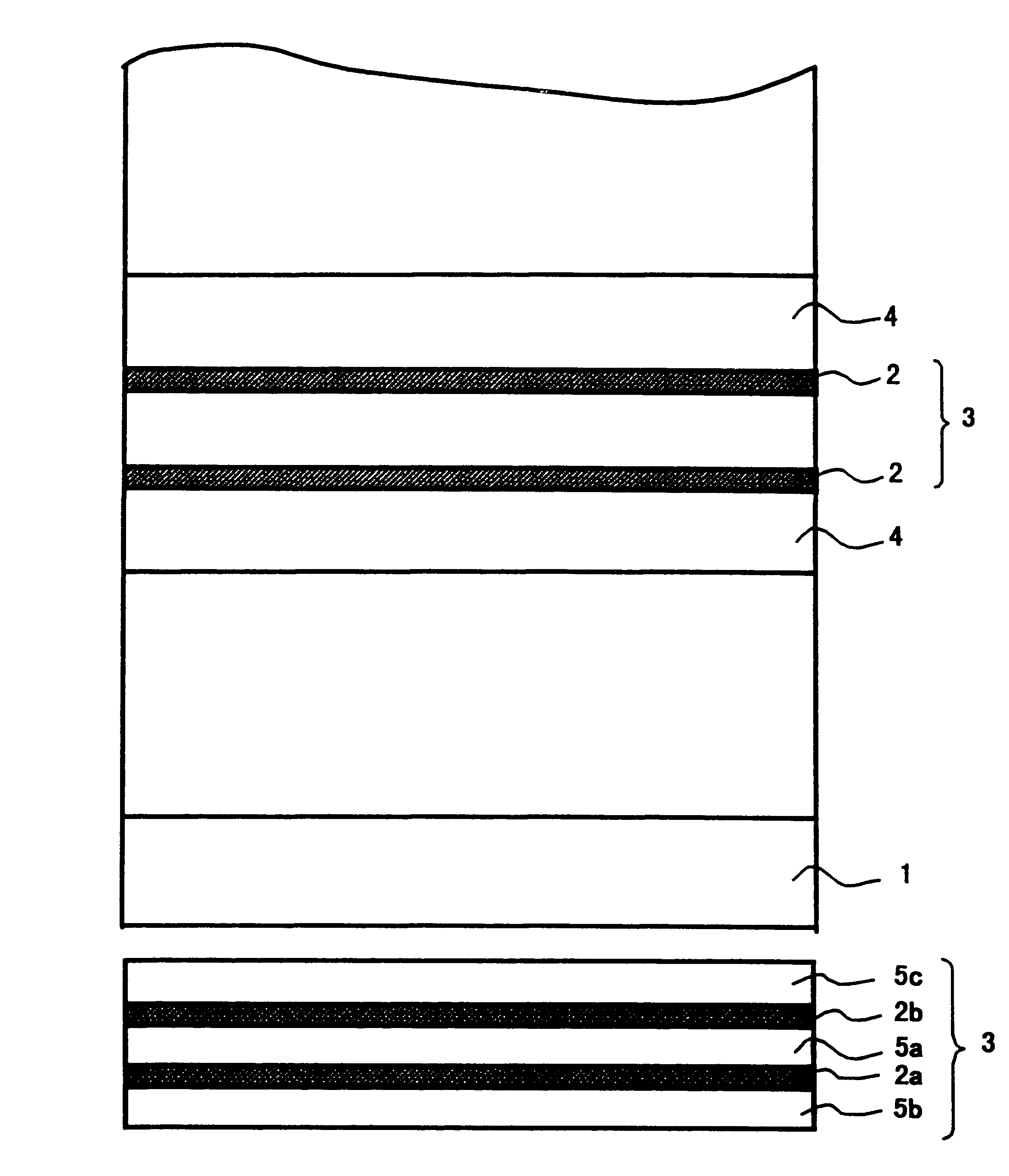
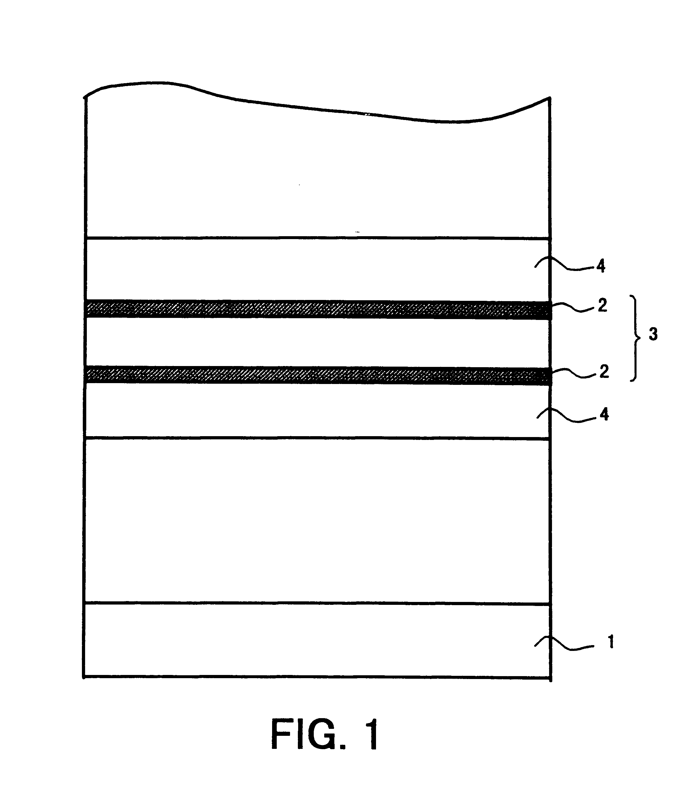
A light emitting device according to the present invention was fabricated as illustrated in FIG. 8. The device was a dielectric-stripe laser incorporating an SCH-DQW (separate confinement heterostructure double quantum well) layer structure.

Referring to FIG. 8, the light emitting device was formed on a (100) n-GaAs substrate 21 with the following layers grown contiguously thereon, in the order recited:

an n-GaAs buffer layer 22,

an n-GaInP(As) lower cladding layer 23 having a thickness of 1.5 micron,

a GaAs light guide layer 24 having a thickness of 100 nm,

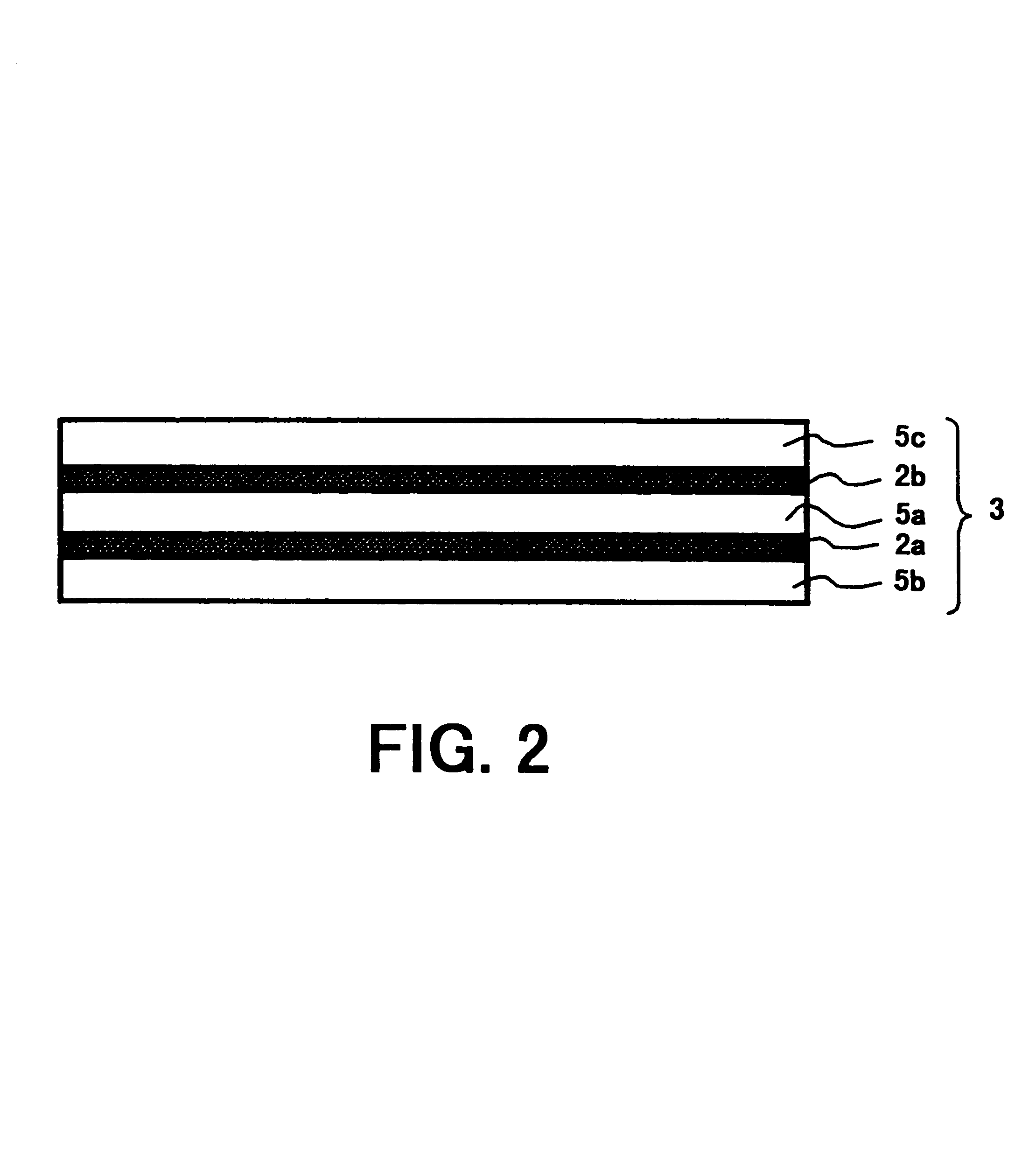
an active (i.e., light emitting) region 27, having a thickness of 13 nm and including Ga.sub.1-x In.sub.x As quantum well layers 25a, 25b and a GaAs barrier layer 26 interposed therebetween;

a GaAs light guide layer 28 having a thickness of 100 nm,

a p-GaInP(As) upper cladding layer 29 having a thickness of 1.5 micron, and

a p-GaAs contact layer 30 having a thickness of 0.3 micron.

Subsequently, the p-GaAs contact layer 30 was subjected ...

example 2

A further light emitting device according to the present invention was fabricated in a manner similar to Example 1, with the exception that the active region included Ga.sub.0.67 In.sub.0.33 No.sub.0.006 As.sub.0.994 quantum well layers and GaAs barrier layers, in place of the Ga.sub.1-x In.sub.x As quantum well layers and GaAs barrier layer of Example 1.

The device was a dielectric-stripe laser incorporating an SCH-DQW layer structure.

Now referring again to FIG. 8, the light emitting device was formed on a (100) n-GaAs substrate with the following layers grown contiguously thereon, in the order recited:

an n-GaAs buffer layer,

an n-GaInP(As) lower cladding layer having a thickness of 1.5 micron,

a GaAs light guide layer having a thickness of 100 nm,

an active region including Ga.sub.0.67 In.sub.0.33 N.sub.0.006 As.sub.0.994 quantum well layers and GaAs barrier layers each having a thickness of 13 nm and interposed therebetween, which were formed in similar manner to those illustrated in...

example 3

A light emitting device according to the present invention was fabricated in a manner similar to Example 2, with the exception that an n-GaAs substrate was used such that the direction normal to the surface thereof was misoriented by approximately 2.degree. from the direction normal to the (100) plane toward the [011] direction, and that the active region comprised Ga.sub.0.6 In.sub.0.4 N.sub.0.005 As.sub.0.995 quantum well layers.

The device was a dielectric-stripe laser incorporating an SCH-DQW layer structure.

Referring again to FIG. 8, the light emitting device was formed on the above-mentioned n-GaAs substrate with the following layers grown contiguously thereon, in the order recited:

an n-GaAs buffer layer,

a n-GaInP(As) lower cladding layer having a thickness of 1.5 micron,

a GaAs light guide layer having a thickness of 100 nm,

an active region including Ga.sub.0.6 In.sub.0.4 N.sub.0.005 As.sub.0.995 quantum well layers and GaAs barrier layers each having a thickness of 13 nm and i...


PUM


Abstract

A semiconductor light emitting device is disclosed, including a semiconductor substrate, an active region comprising a strained quantum well layer, and a cladding layer for confining carriers and light emissions, wherein the amount of lattice strains in the quantum well layer is in excess of 2% against either the semiconductor substrate or cladding layer and, alternately, the thickness of the quantum well layer is in excess of the critical thickness calculated after Matthews and Blakeslee.

Description

1. FieldThis specification relates to layered semiconductor structures and more particularly, to light emitting devices incorporating layered III-V alloy semiconductor structures for use in durable laser diodes having light emissions of longer wavelengths, and apparatus and system using such light emitting devices.2. Description of the Related ArtAs communication systems have developed and both desired and current information transmission rates have increased, more attention has been focused on the development of optical communication systems.As presently contemplated, the optical communication system presently used in main communication lines will be extended to each subscriber's domestic line. To implement such systems, it is indispensable to develop smaller and less expensive optical devices such as, among others, light emitting devices like laser diodes and light emitting diodes and photoreceptors.Light emitting devices such as laser diodes are conventionally accompanied by a co...

Claims


Application Information

Patent Timeline
Patent Type & Authority Patents(United States)
IPC IPC(8): H01L33/00H01S5/34H01S5/00H01S5/323H01S5/343H01S5/183H01L33/06
CPCB82Y20/00H01L33/06H01S5/18311H01S5/34H01S5/18305H01S5/18341H01S5/18358Y10S257/918H01S5/32358H01S5/32366H01S5/3403H01S5/34306H01S2301/176H01S5/18369
Inventor SATO, SHUNICHITAKAHASHI, TAKASHIJIKUTANI, NAOTO
Owner RICOH KK
Why Eureka
Try Eureka