Method of manufacturing thin film device

a thin film, manufacturing method technology, applied in the direction of dielectric characteristics, other domestic objects, chemistry apparatus and processes, etc., can solve the problems of difficult to ensure high performance by using the functional unit, damage to the permanent substrate, etc., to improve the reliability of the device and simplify the process

Inactive Publication Date: 2010-03-04
SAMSUNG ELECTRO MECHANICS CO LTD
View PDF6 Cites 23 Cited by
  • Summary
  • Abstract
  • Description
  • Claims
  • Application Information

AI Technical Summary

Benefits of technology

[0012]An aspect of the present invention provides a method of manufacturing a thin film device that simplifies a process and imp...

Problems solved by technology

However, since it is difficult to ensure high performance by using the functional unit formed of the organic thin film, an inorganic material, such as polysilicon (poly-Si) or an oxide thin film, is used to form a functional unit of the flexible device.
Here, since it is difficult to directly apply the high-temperature semiconductor film forming technique to the flexible substrate formed of the organic material, the thin-film transfer technique that transfers a thin film formed of an inorganic material, such as a semiconduc...

Method used


Image

  • Method of manufacturing thin film device
  • Method of manufacturing thin film device
  • Method of manufacturing thin film device

Examples


Embodiment Construction

[0032]Exemplary embodiments of the present invention will now be described in detail with reference to the accompanying drawings.

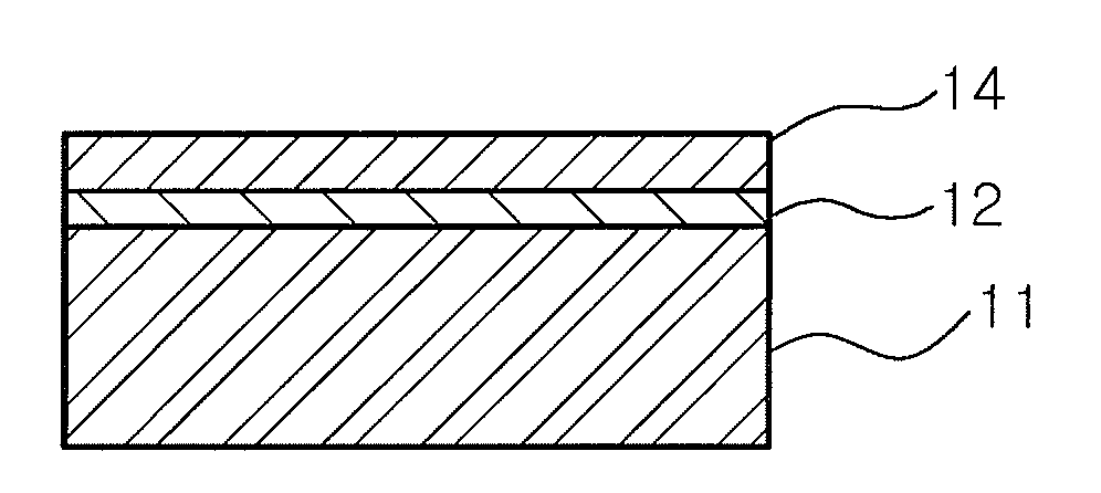
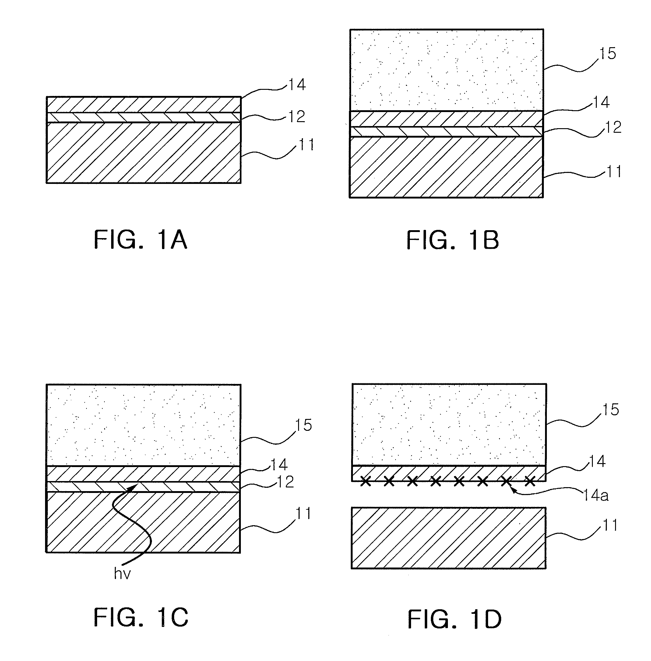
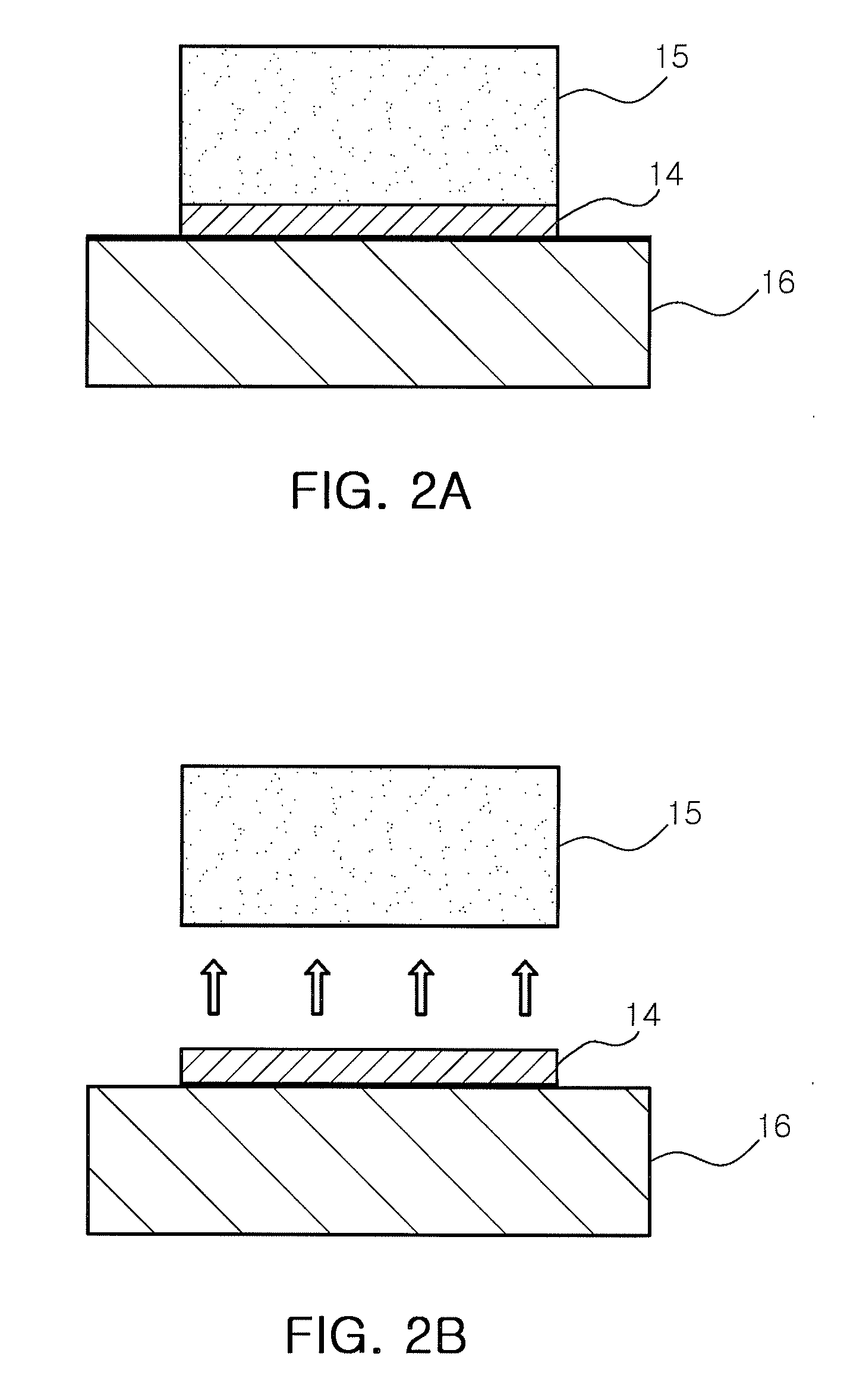
[0033]FIGS. 1A through 1D are cross-sectional views illustrating a process of forming a lamination including a transfer object in a method of manufacturing a thin film device according to an exemplary embodiment of the invention.

[0034]As shown in FIG. 1A, a sacrificial layer 12 and a thin film 14 to be transferred are sequentially formed on a first substrate 11.

[0035]A thin film 14 is formed on the first substrate 11. The first substrate 11 is formed of a material having durability in a high-temperature film forming process of growing the desired thin film 14. In general, a laser lift off (LLO) method is used for the separation of the thin film 14 to be transferred. This is also considered when selecting the material forming the first substrate 11.

[0036]That is, the first substrate 11 may be formed of a material having a larger band gap energy than a band ...


PUM

PropertyMeasurementUnit
Flexibilityaaaaaaaaaa
Areaaaaaaaaaaa
Transparencyaaaaaaaaaa

Abstract

A method of manufacturing a thin film device according to an aspect of the invention may include: forming a sacrificial layer on a first substrate; forming a thin film on the sacrificial layer, the thin film being an object of transfer; temporarily bonding a support structure to the thin film; removing the sacrificial layer to separate the thin film from the first substrate; bonding the thin film, temporarily bonded to the support structure, to a second substrate; and separating the support structure from the thin film.

Description

CROSS-REFERENCE TO RELATED APPLICATIONS[0001]This application claims the priority of Korean Patent Application No. 2008-0086469 filed on Sep. 2, 2008, in the Korean Intellectual Property Office, the disclosure of which is incorporated herein by reference.BACKGROUND OF THE INVENTION[0002]1. Field of the Invention[0003]The present invention relates to a method of manufacturing a thin film device, and more particularly, to a method of manufacturing a thin film device using a thin-film transfer process that can be used as a technique for manufacturing a flexible substrate.[0004]2. Description of the Related Art[0005]In general, a thin-film transfer technique has been widely used in thin film devices, such as thin film transistors (TFTs), electronic devices, and optical devices including organic EL devices.[0006]The thin-film transfer technique generally refers to a technique that forms a predetermined thin film on a preliminary substrate and then transfers the thin film onto a permanent...

Claims


Application Information

Patent Timeline
IPC IPC(8): B32B37/02
CPCB32B37/025B32B38/06B32B2310/0843B32B2457/20H01L29/78603H05K3/1275H05K2203/107H05K3/386H05K2201/0108H05K2201/0317H05K2203/016H05K2203/0534H05K3/20
Inventor LEE, HWAN-SOOOH, YONGSOO
Owner SAMSUNG ELECTRO MECHANICS CO LTD
Why Eureka
Try Eureka