

Capacitor insulating film, method of forming the same, capacitor and semiconductor device using the capacitor insulating film
a technology of capacitor insulating film and sto film, which is applied in the direction of fixed capacitor dielectric, fixed capacitor details, fixed capacitors, etc., can solve the problems of large capacity of capacitors, difficult to make sto film thick, and difficulty in acquiring a sufficient capacity of capacitors
- Summary
- Abstract
- Description
- Claims
- Application Information
AI Technical Summary
Problems solved by technology
Method used
Image

Examples
first preferred embodiment
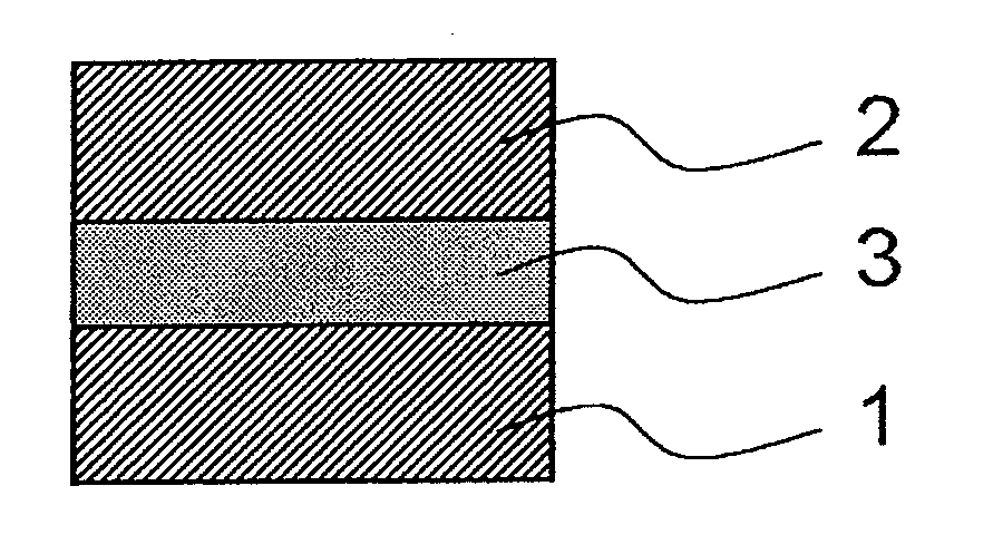
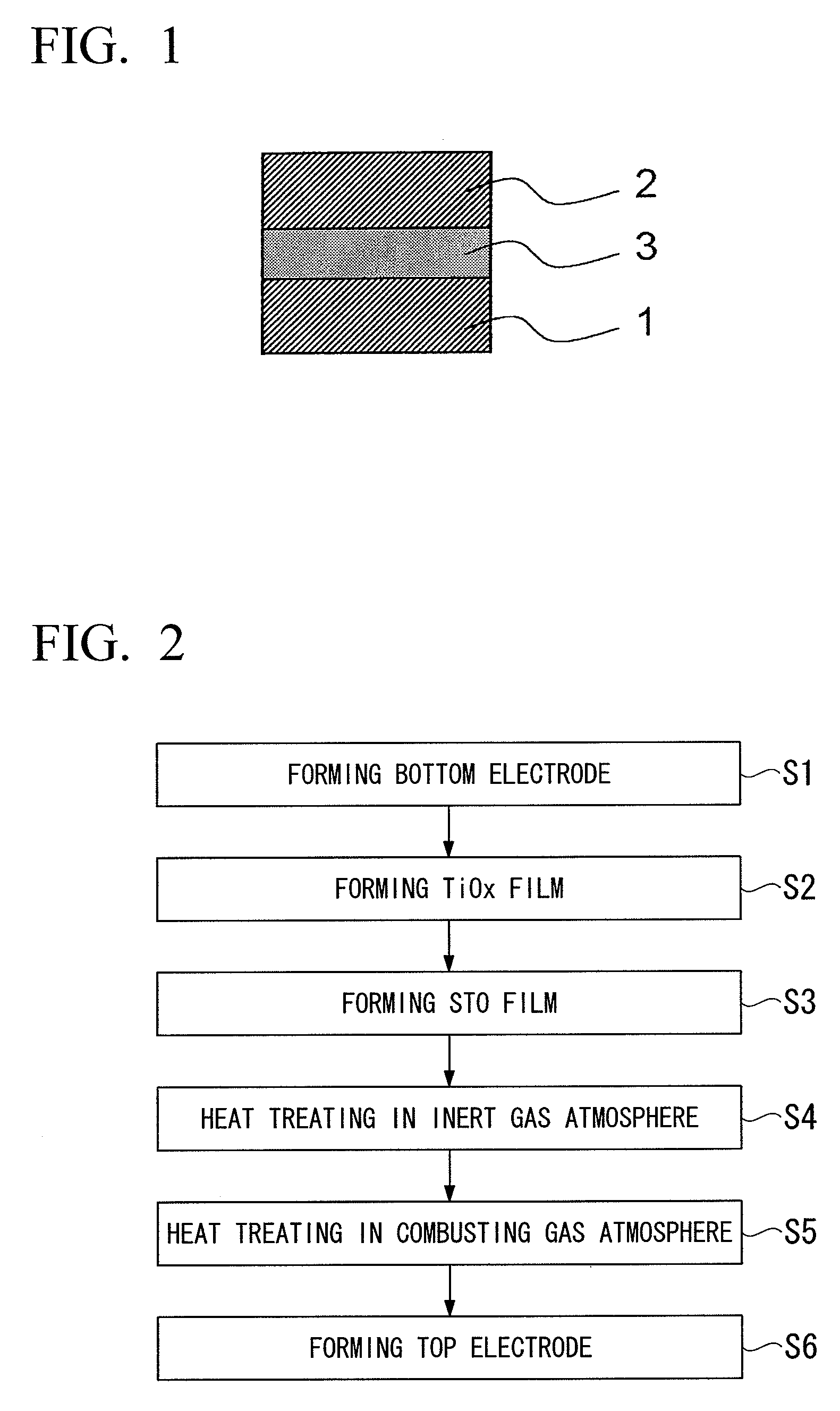
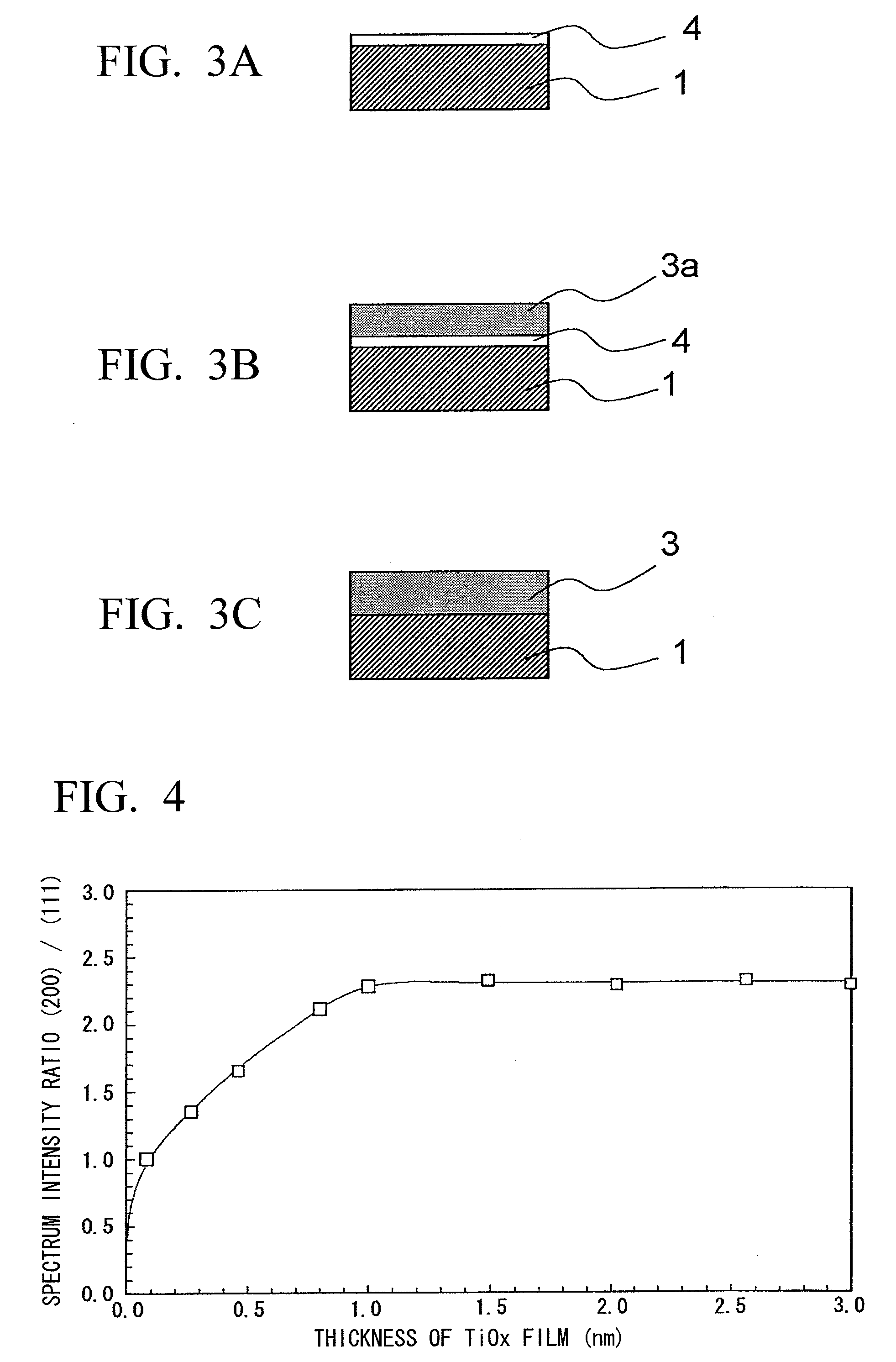
[0036]FIG. 1 is a fragmentary cross sectional elevation view illustrating a capacitor in accordance with a first preferred embodiment of the present invention. The capacitor is formed by disposing a crystal STO film 3 between electrodes 1 and 2 that are made of a ruthenium (Ru). The STO film 3 is formed so that the spectrum intensity ratio (200) / (111) of the STO film 3 is in the range of 1.0 to 2.3, where the spectrum intensity ratio (200) / (111) of the STO film 3 is the ratio of the spectrum intensity of (200) crystal face of the STO film 3 to the spectrum intensity of (111) crystal face of the STO film 3, and each of the spectrum intensities of the (200) crystal face and (111) crystal face is measured by the X-ray diffraction method.
[0037]A material of the electrodes 1 and 2 is not limited to the ruthenium, but may be other metal film of high melting point such as a platinum (Pt) film or a titanium nitride (TiN) film, or a laminated film made of a plurality of metal films of high m...
second preferred embodiment
[0057]The capacitor that uses the capacitor insulating film of the present invention can be applicable not only to the case when the electrode has a two-dimensional structure described in the first embodiment but also to the case when the electrode has a three-dimensional structure.
[0058]The capacitor having three-dimensional structure will be described by referring FIGS. 8A and 8B.
[0059]FIG. 8A is a fragmentary vertical cross-sectional view illustrating the capacitor of a circular cylindrical shape that is a pillar shape. The capacitor includes the bottom electrode 10, the capacitor insulating film 11 of the present invention, and the top electrode 12. The bottom electrode 10 of the capacitor is formed in the circular cylindrical shape that is the pillar shape using a metal with a high melting point such as the ruthenium (Ru). The capacitor insulating film 11 is the STO film that is formed so as to cover the top surface and the side surface of the bottom electrode 10 by the above d...
third preferred embodiment
[0062]The third embodiment that applies the capacitor insulating film of the present invention to the capacitor in the memory cell of the DRAM will be described. The third embodiment is an example of the semiconductor device using the capacitor insulating film of the present invention.
[0063]FIG. 9 is a fragmentary plain view illustrating the memory cell of the DRAM. Only a part of the memory cell is illustrated in FIG. 9 for description.
[0064]A plurality of active regions 103 are disposed on a semiconductor substrate in a regular cycle. The semiconductor substrate is not illustrated in the figure. The plurality of active regions 103 are districted by a plurality of device isolation regions 102. Each of the device isolation regions 102 is formed by embedding an insulating film such as a silicon dioxide film in the semiconductor substrate using a known method. A plurality of gate electrodes 106 are disposed across the plurality of active regions 103. Each of the plurality of gate elec...
PUM
| Property | Measurement | Unit |
|---|---|---|
| Temperature | aaaaa | aaaaa |
| Temperature | aaaaa | aaaaa |
| Temperature | aaaaa | aaaaa |
Abstract
Description
Claims
Application Information