High speed flash memory

a flash memory and high-speed technology, applied in the field of integrated circuits, can solve the problems of difficult timing generation for controlling the latch, low turn-on current through the floating gate mos transistor, and difficulty in obtaining the necessary current to measure the stored data in the memory cell, etc., to achieve easy control, reduce current difference, and sense the time

Inactive Publication Date: 2010-03-04
KIM JUHAN
View PDF8 Cites 18 Cited by
  • Summary
  • Abstract
  • Description
  • Claims
  • Application Information

AI Technical Summary

Benefits of technology

[0015]And, amplifying transistors of the sense amps are composed of relatively long channel transistors than those of pre-charge transistors in order to reduce turn-off current, which reduces power consumption.
[0017]Furthermore, configuring the memory is more flexible, such that number of sense amps can be determined by the target speed. For example, high speed application needs more segmented array with more sense amps, while high density application needs more memory cells with reduced number of sense amps, thus cell efficiency is increased.
[0020]More specifically, a reference signal is generated by one of fast changing data, such as low threshold data, with high gain from reference cells, which signal serves as a reference signal to generate a locking signal for an output latch circuit in order to reject latching another data, such as, high threshold data, which is slowly changed with low gain, so that low threshold data (in a charge trap region) is arrived first while high threshold data is arrived later. The time-domain sensing scheme effectively differentiates low threshold data and high threshold data with time delay control, while the conventional sensing scheme is current-domain or voltage-domain sensing scheme. In the convention memory, the selected memory cell charges or discharges a long and heavy bit line, and the changed voltage of the bit line is compared by a latch which determines an output at a time. In the present invention, there are many advantages to realize the time-domain sensing scheme, so that the sensing time is easily controlled by a tunable delay circuit, which compensates cell-to-cell variation and wafer-to-wafer variation, such that there is a need for adding a delay time before locking the output latch circuit with a statistical data for all the memory cells, such as mean time between fast data and slow data. Thereby the tunable delay circuit generates a delay for optimum range of locking time. And a read output from the memory cell is transferred to the output latch circuit through a returning read path, thus the access time is equal regardless of the location of the selected memory cell, which is advantageous to transfer the read output to the external pad at a time.
[0021]Furthermore, the time-domain sensing scheme is useful for reducing the cell current difference between the turn-on current of the low threshold data and the turn-off current of the high threshold data. In the conventional flash memory, there is at least several 1000 times difference between the turn-on current and the turn-off current, in order to read the memory cell with existing comparator or an inverter latch through heavy bit line. In the present invention, the current difference can be reduced, for example, to several 100 times instead of several 1000 times, as long as the distribution of the difference is stable at a given fabrication process for manufacturing because lightly loaded bit line can be driven by the weak memory cell through multi-stage sense amps in the time domain, which means that the memory cell can be miniaturized further.

Problems solved by technology

The conventional flash memory has progressed its miniaturization and as a result there arises difficulties in obtaining necessary current to measure the stored data in the memory cell.
When the ratio is very low, the leakage current (turn-off current) may also discharge the bit line, which may cause the sensing error because the latch node is discharged whether the threshold voltage of the memory cell is low or high.
And also the timing generation for controlling the latch is more difficult because there is no precise timing generator based on the turn-on current.
Furthermore, one of major problem is that the turn-on current through the floating gate MOS transistor is low, around 1 uA or less for the conventional flash memory, as published, “A 90-nm CMOS 1.8-V 2-Gb NAND Flash Memory for Mass Storage Applications”, IEEE Journal of Solid-State Circuits. Vol. 38, No. 11, November 2003.

Method used


Image

  • High speed flash memory
  • High speed flash memory
  • High speed flash memory

Examples


Embodiment Construction

)

[0041]Reference is made in detail to the preferred embodiments of the invention. While the invention is described in conjunction with the preferred embodiments, the invention is not intended to be limited by these preferred embodiments. On the contrary, the invention is intended to cover alternatives, modifications and equivalents, which may be included within the spirit and scope of the invention as defined by the appended claims. Furthermore, in the following detailed description of the invention, numerous specific details are set forth in order to provide a thorough understanding of the invention. However, as is obvious to one ordinarily skilled in the art, the invention may be practiced without these specific details. In other instances, well-known methods, procedures, components, and circuits have not been described in detail so that aspects of the invention will not be obscured.

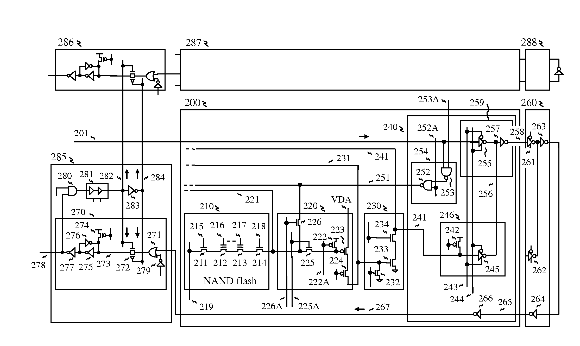
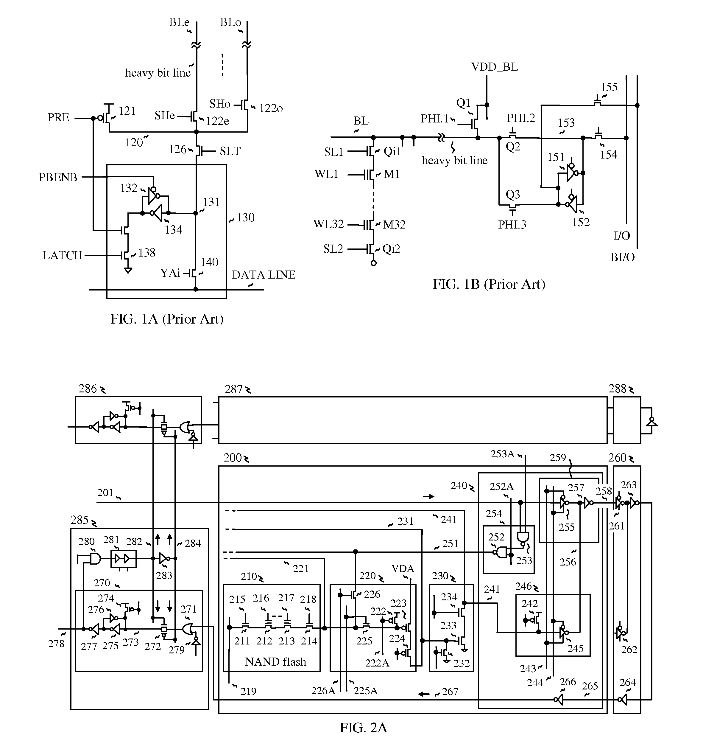
[0042]The present invention is directed to NAND flash memory with light bit line architecture, as s...


PUM


Abstract

For realizing high speed flash memory, bit line is multi-divided for reducing parasitic capacitance, so that local bit line is quickly discharged when reading a memory cell and multi-stage sense amps are used, wherein the multi-stage sense amps are composed of a first dynamic circuit serving as a local sense amp connecting to the local bit line through a read transistor, a second dynamic circuit serving as a segment sense amp for reading the local sense amp, and a tri-state inverter serving as an amplify circuit of a global sense amp for reading the segment sense amp. When reading data, a cell current difference is converted to a time difference for differentiating low threshold data and high threshold data by the multi-stage sense amps. And a buffered data path is connected to the global sense amp for achieving fast data transfer. Additionally, alternative circuits and memory cell structures are described.

Description

FIELD OF THE INVENTION[0001]The present invention relates generally to integrated circuits, in particular to high speed flash memory with light bit line architecture, such as, NAND flash memory and NOR flash memory.BACKGROUND OF THE INVENTION[0002]Flash memory device includes charges, wherein charges are stored in an isolated conductor, commonly referred to as a floating gate, in an FET (field-effect transistor) device. A memory cell (cell transistor) operates by storing electric charge (representing either a binary “0” or “1” state of one data bit) on the floating gate, which is incorporated into a MOS (Metal-Oxide Semiconductor) field-effect transistor. The stored charges affect the VT (threshold voltage) of the transistor, thereby providing a way to read the current through the storage device.[0003]A memory cell typically consists of a transistor, a floating gate, and a control gate above the floating gate in a stacked gate structure. The floating gate, typically composed of poly...

Claims


Application Information

Patent Timeline
Patent Type & Authority Applications(United States)
IPC IPC(8): G11C16/04G11C16/06G11C7/00
CPCG11C7/067G11C7/18G11C11/5642G11C16/0483G11C16/10H01L27/11551G11C16/26G11C16/32H01L27/11519H01L27/11526G11C16/24H10B41/10H10B41/40H10B41/20
Inventor KIM, JUHAN
Owner KIM JUHAN
Why Eureka
Try Eureka