Method and system for monolithic integration of photonics and electronics in CMOS processes

a technology applied in the field of monolithic integration of photonics and electronics in cmos processes, can solve the problems of cable bulk penalties, large power requirements, and complex structure, and achieve only modest improvements in reach and limited scalability

Active Publication Date: 2010-03-11
CISCO TECH INC
View PDF14 Cites 102 Cited by
  • Summary
  • Abstract
  • Description
  • Claims
  • Application Information

AI Technical Summary

Benefits of technology

[0008]A system and/or method for monolithic integration of photonics and electronics in CMOS processes, substantiall...

Problems solved by technology

They can be mitigated to some extent with equalization, coding, and shielding, but these techniques require considerab...

Method used


Image

  • Method and system for monolithic integration of photonics and electronics in CMOS processes
  • Method and system for monolithic integration of photonics and electronics in CMOS processes
  • Method and system for monolithic integration of photonics and electronics in CMOS processes

Examples


Embodiment Construction

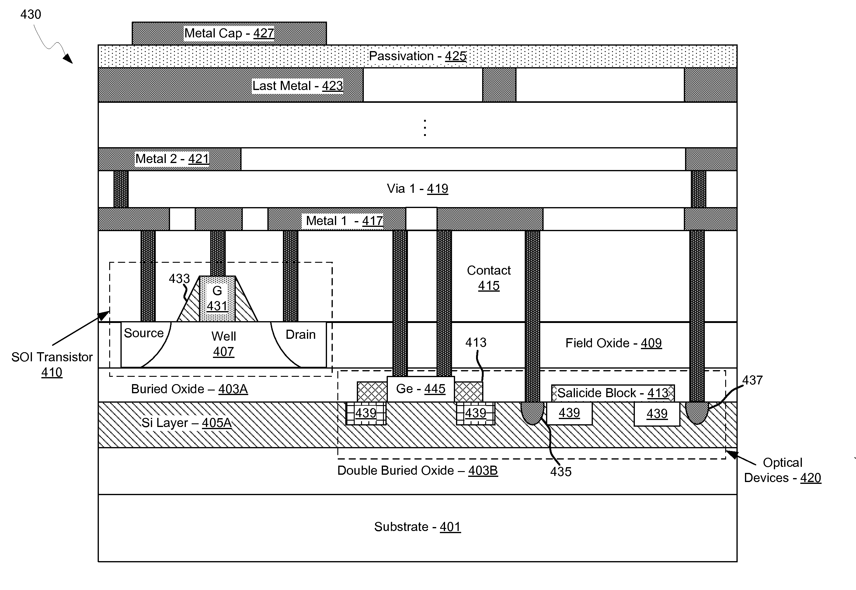
[0028]Certain aspects of the invention may be found in a method and system for monolithic integration of photonics and electronics in CMOS processes. Exemplary aspects of the invention may comprise fabricating photonic and electronic devices on a single complementary metal-oxide semiconductor (CMOS) wafer with different silicon layer thicknesses for the photonic and the electronic devices. The electronic and photonic devices may be fabricated on a semiconductor-on-insulator (SOI) wafer utilizing a bulk CMOS process. The electronic and photonic devices may be fabricated on a SOI wafer utilizing a SOI CMOS process. The different silicon layer thicknesses may be fabricated utilizing a double SOI process and / or a selective area growth process. Cladding layers for the photonic devices may be fabricated utilizing one or more oxygen implants into the CMOS wafer and / or utilizing CMOS trench oxide on the CMOS wafer. Silicon material for the photonic devices may be deposited on the CMOS trenc...


PUM


Abstract

Methods and systems for monolithic integration of photonics and electronics in CMOS processes are disclosed and may include fabricating photonic and electronic devices on a single CMOS wafer with different silicon layer thicknesses. The devices may be fabricated on a semiconductor-on-insulator (SOI) wafer utilizing a bulk CMOS process and/or on a SOI wafer utilizing a SOI CMOS process. The different thicknesses may be fabricated utilizing a double SOI process and/or a selective area growth process. Cladding layers may be fabricated utilizing one or more oxygen implants and/or utilizing CMOS trench oxide on the CMOS wafer. Silicon may be deposited on the CMOS trench oxide utilizing epitaxial lateral overgrowth. Cladding layers may be fabricated utilizing selective backside etching. Reflective surfaces may be fabricated by depositing metal on the selectively etched regions. Silicon dioxide or silicon germanium integrated in the CMOS wafer may be utilized as an etch stop layer.

Description

CROSS-REFERENCE TO RELATED APPLICATIONS / INCORPORATION BY REFERENCE[0001]This application makes reference to and claims priority to U.S. Provisional Application Ser. No. 61 / 191,479 filed on Sep. 8, 2008, and Provisional Application Ser. No. 61 / 199,353 filed on Nov. 14, 2008, which are hereby incorporated herein by reference in their entirety.[0002]Each of the above stated applications is hereby incorporated herein by reference in its entirety.FEDERALLY SPONSORED RESEARCH OR DEVELOPMENT[0003][Not Applicable]MICROFICHE / COPYRIGHT REFERENCE[0004][Not Applicable]FIELD OF THE INVENTION[0005]Certain embodiments of the invention relate to semiconductor processing. More specifically, certain embodiments of the invention relate to a method and system for monolithic integration of photonics and electronics in CMOS processes.BACKGROUND OF THE INVENTION[0006]As data networks scale to meet ever-increasing bandwidth requirements, the shortcomings of copper data channels are becoming apparent. Signa...

Claims


Application Information

Patent Timeline
IPC IPC(8): H01L27/12H01L21/782
CPCH01L27/1203H01L21/84H01L2225/06541H01L25/167H01L25/0652H04B10/40H01L27/0688H04B10/2575
Inventor PINGUET, THIERRYGLOECKNER, STEFFENDE DOBBELAERE, PETERABDALLA, SHERIFKUCHARSKI, DANIELMASINI, GIANLORENZOYOKOYAMA, KOSEIGUCKENBERGER, JOHNMEKIS, ATTILA
Owner CISCO TECH INC
Why Eureka
Try Eureka