Semiconductor integrated circuit device

a technology of integrated circuits and semiconductors, applied in semiconductor devices, semiconductor/solid-state device details, diodes, etc., can solve the problems of weak structural strength of soi devices, easy breakage of internal elements, and disadvantageous extension of protection circuits and chip areas, so as to reduce leak current, reduce the gate length of protection nmos transistors, and high esd breakdown strength

Inactive Publication Date: 2006-02-02
SEIKO INSTR INC
View PDF9 Cites 18 Cited by
  • Summary
  • Abstract
  • Description
  • Claims
  • Application Information

AI Technical Summary

Benefits of technology

[0025] As set forth above, in the semiconductor integrated circuit device, the gate electrode of the NMOS transistor as an internal element formed on the semiconductor thin film has N-type conductivity, while the gate electrode of the protection NMOS transistor as an ESD input / output protection element formed on the semiconductor support substrate has P-type conductivity, making it possible to reduce leak current and to shorten the gate length of the protection NMOS transistor. Ensuring a high ESD breakdown strength owing to the formation on the support substrate, the protection NMOS transistor absorbs ESD noise first to protect an input / output terminal of the internal element on the semiconductor thin film, which is weak against the ESD noise, especially, to protect the output terminal. In particular, a protection effect can be greatly exerted in a power management semiconductor integrated circuit device or analog semiconductor integrated circuit device in which electrical input / output characteristics are important.

Problems solved by technology

As a result, an SOI device is structurally weak against ESD.
As mentioned above, the formation of the ESD protection element on the SOI substrate involves enlarging the protection element or increasing the number of protection elements for attaining a sufficient ESD strength, and is disadvantageous in extension of the protection circuit and chip area.
However, when the semiconductor thin film or buried insulating film of the SOI substrate is partially removed to expose the semiconductor support substrate, and the protection element is formed on the exposed portion, the protection element itself can secure a sufficient ESD strength but a problem comes out that the internal element easily breaks down.
However, when the withstand voltage of the ESD protection element on the semiconductor support substrate is too high, the protection element cannot react to the ESD noise introduced from the output terminal 302, and the noise enters the internal element on the SOI semiconductor thin film resulting in the breakdown of the internal element.

Method used


Image

  • Semiconductor integrated circuit device
  • Semiconductor integrated circuit device
  • Semiconductor integrated circuit device

Examples


Embodiment Construction

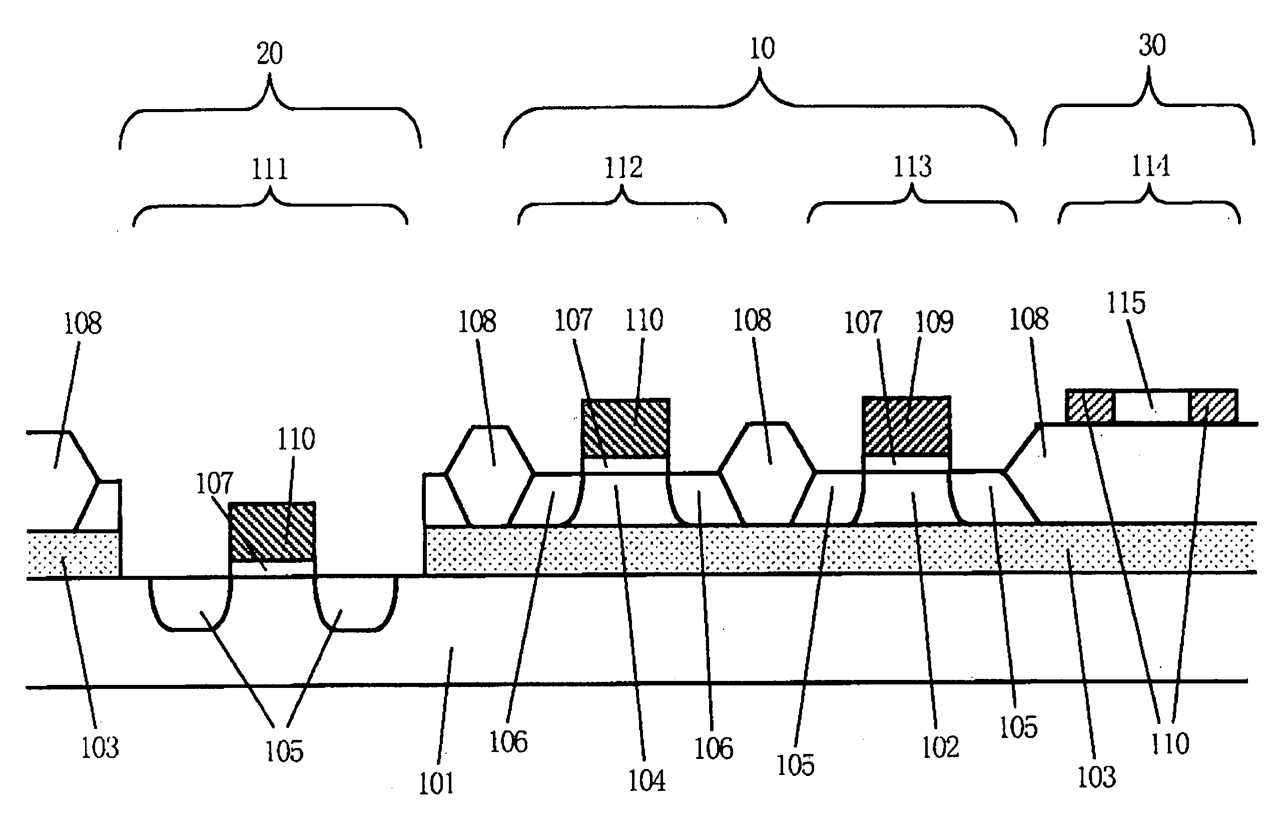
[0036] Hereinafter, embodiments of the present invention will be described in detail with reference to the accompanying drawings. FIG. 1 is a schematic sectional diagram showing a semiconductor integrated circuit device according to an embodiment of the present invention.

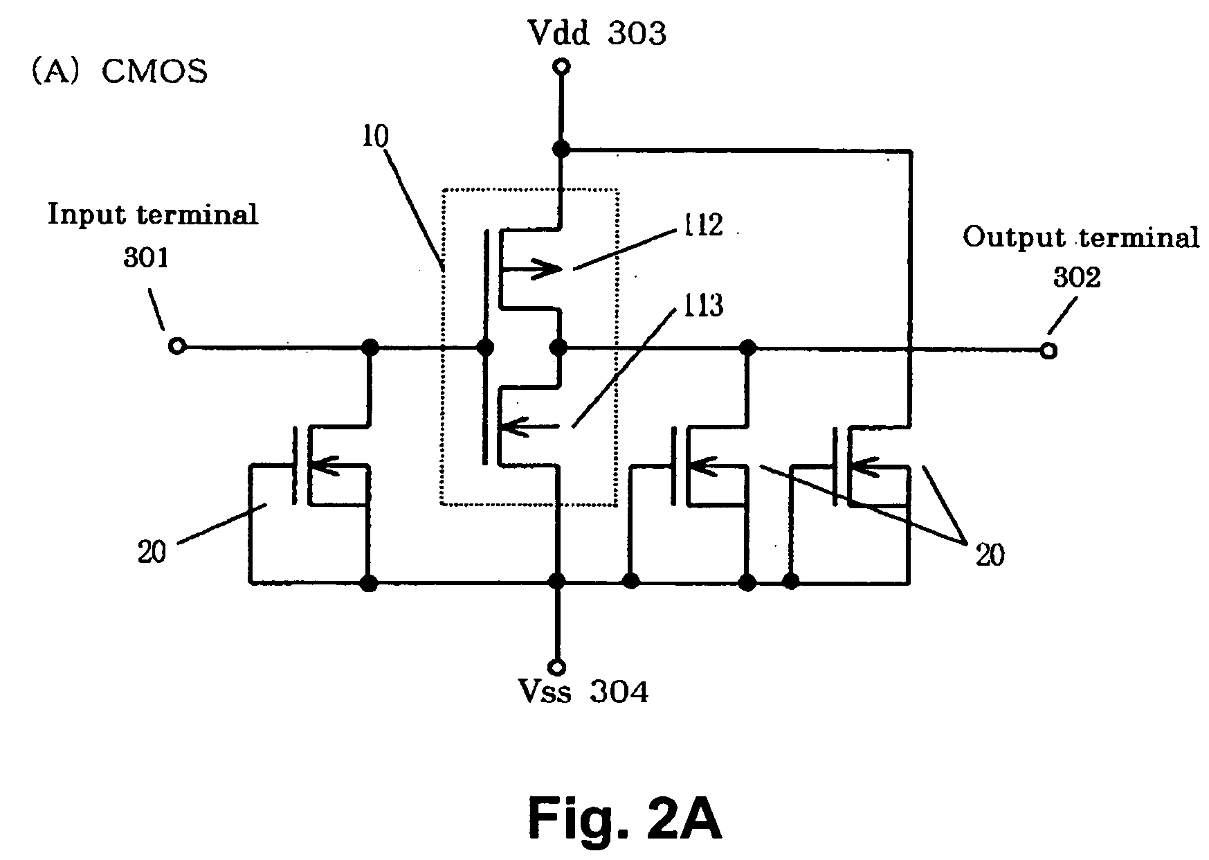
[0037] A silicon-on-insulator (SOI) substrate is composed of, for example, a semiconductor support substrate 101 of a P-type conductivity, which is made of single crystal, a buried insulating film 103, and a semiconductor thin film 102 of a P-type conductivity, which is made of single crystal and is used to form elements. Formed on the P-type semiconductor thin film 102 are a CMOS inverter as an internal element 10 composed of a first N-channel MOS transistor (hereinafter abbreviated to “NMOS”) 113 and a first P-channel MOS transistor (hereinafter abbreviated to “PMOS”) 112, and a P− resistor 114 made of polysilicon as a resistor element 30. However, the internal element 10 is not limited to the CMOS inverter but c...


PUM


Abstract

Provided is a structure in which a gate electrode of an MMOS transistor of a fully depleted SOT CMOS circuit formed on a semiconductor thin film has an N-type conductivity, while a gate electrode of an protection NMOS transistor as an ESD input/output protection element formed on a semiconductor support substrate has a P-type conductivity, making it possible to protect input/output terminals, especially, an output terminal of a fully depleted SOI CMOS device, which is weak against ESD noise, while ensuring a sufficient ESD breakdown strength.

Description

BACKGROUND OF THE INVENTION [0001] 1. Field of the Invention [0002] The present invention relates to a semiconductor integrated circuit device, in particular, to an electrostatic discharge (ESD) protection device for SOI structure. [0003] 2. Description of the Related Art [0004] In a semiconductor integrated circuit device including a resistor circuit composed of a resistor made of polysilicon or the like, an input or output protection element made up of a diode or a MOS transistor is generally disposed between an internal circuit and an external input / output terminal to prevent breakdown of internal elements composing the internal circuit when an excess amount of current flows into the circuit from outside by static electricity. [0005]FIGS. 2A to 2C show examples of an input / output circuit unit in a conventional semiconductor integrated circuit device having such protection circuits. In FIG. 2A, a CMOS inverter composed of an N-channel MOS transistor 113 and a P-channel MOS transis...

Claims


Application Information

Patent Timeline
Patent Type & Authority Applications(United States)
IPC IPC(8): H01L23/62
CPCH01L27/0266H01L27/1203H01L27/0629H01L27/04
Inventor HASEGAWA, HISASHIYOSHIDA, YOSHIFUMI
Owner SEIKO INSTR INC
Why Eureka
Try Eureka