Semiconductor integrated circuit device

Inactive Publication Date: 2007-06-21
ABLIC INC
View PDF26 Cites 19 Cited by
  • Summary
  • Abstract
  • Description
  • Claims
  • Application Information

AI Technical Summary

Benefits of technology

[0029] As described above, in the semiconductor integrated circuit device, the source region of the N-channel transistor as an internal element formed on the semiconductor thin film has a polygonal shape and opposes to only one side of the drain region which also has a polygonal shape, while the source region of the ESD input/output protection element having N-type MOS structure formed on the semiconductor support substrate is surrounded by the drain region, resulting easy control of bipolar operating voltage and low withstand voltage of the protection element against

Problems solved by technology

In general, a device element formed on an SOI substrate, particularly on a thin-film SOI substrate, is surrounded by a buried insulating film and an isolation insulating film, and thus exhibits poor heat dissipation performance and is likely to break down by heat generation due to an overcurrent.
Therefore, an SOI device has a structure which is significantly vulnerable to ESD.
When an ESD protection element is formed on the SOI semiconductor thin film to protect an inner circuit, the heat generation due to the over current also causes the protection element easily to break down.
As mentioned above, the formation of the ESD protection element on the SOI substrate involves enlarging the protection element or increasing the number of protection elements for attaining a sufficient ESD st

Method used


Image

  • Semiconductor integrated circuit device
  • Semiconductor integrated circuit device
  • Semiconductor integrated circuit device

Examples


first embodiment

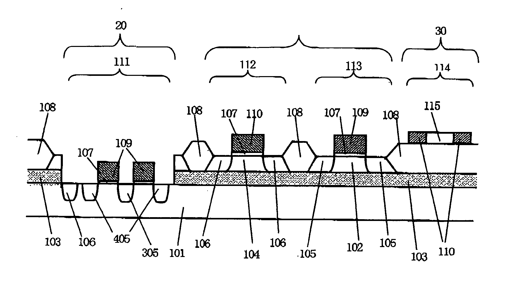
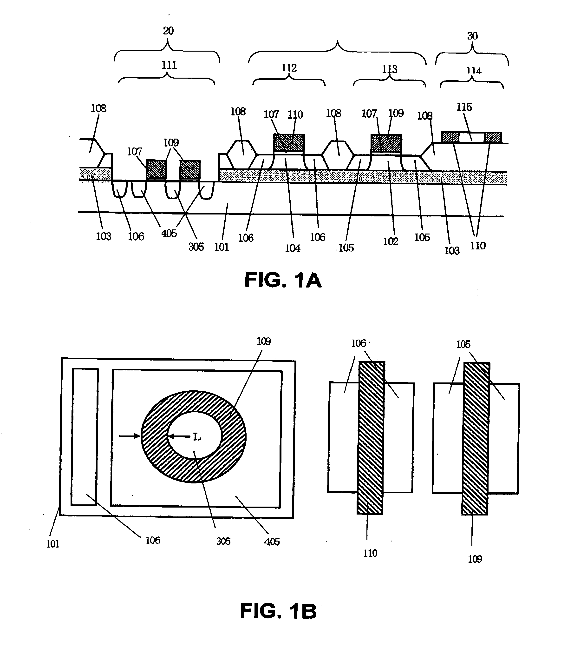
[0057]FIG. 1B is a schematic plan diagram of the semiconductor integrated circuit device shown in FIG. 1A according to the For ease of explanation, a resistor element is not shown in the drawing.

[0058] The NMOS transistor 113 and the PMOS transistor 112 of the internal element each include a source / drain region having a polygonal configuration (although the region is a rectangle in the drawing, polygonal configuration having more than four sides may be adopted), In general, a layout in which one side of the source region faces one side of the drain region is employed. On the other hand, the source 305 of the protection NMOS transistor 111 has a circular configuration and the drain 405 is formed so as to surround the source 305. In other words, the minimum distance between the source 305 and the drain 405 is kept constant. Note that the shape of the source 305 of the protection NMOS transistor 111 is not limited to the circular configuration. The source 305 may have an elliptical or...

second embodiment

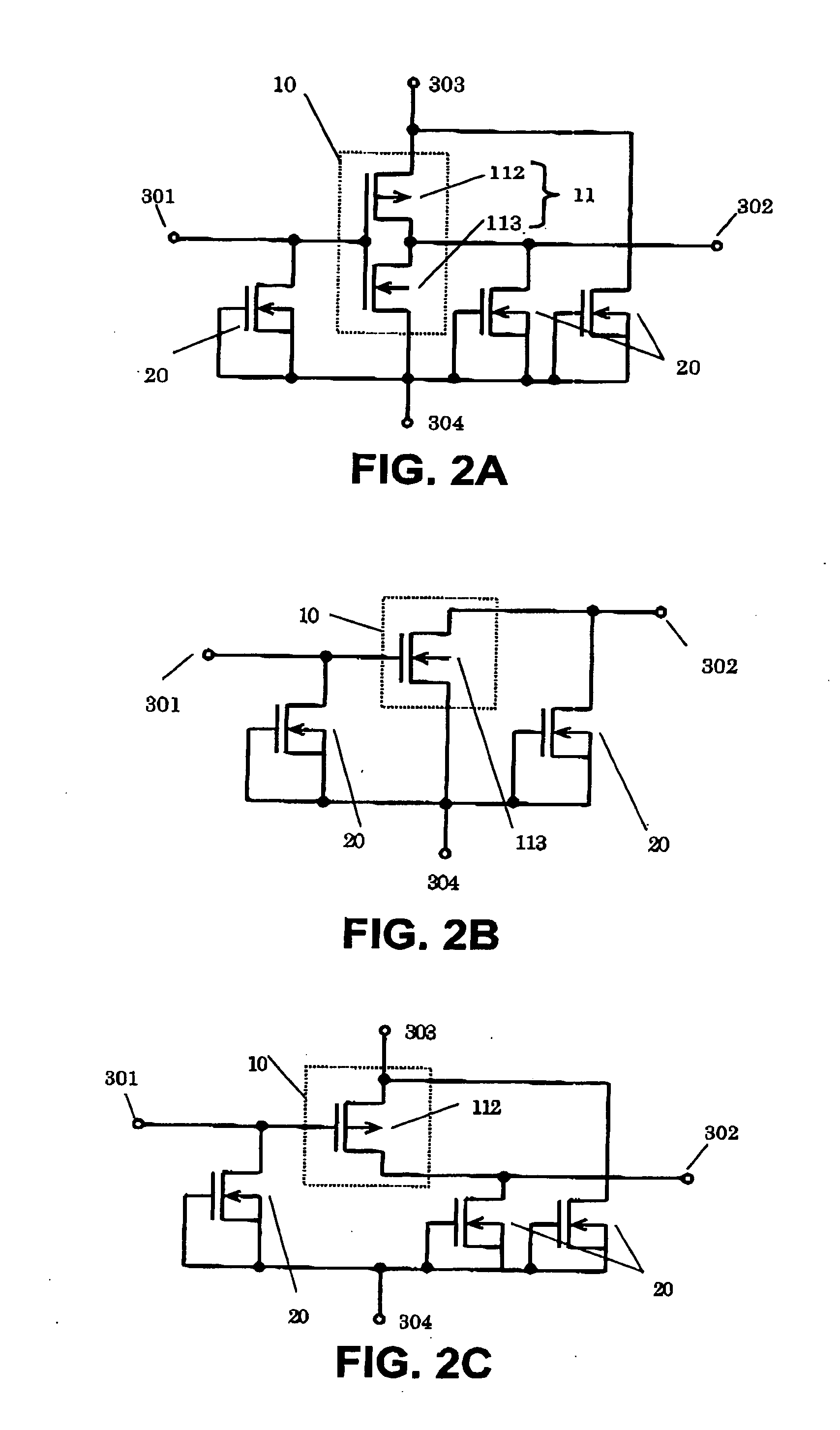
[0061]FIG. 3 is a schematic sectional diagram showing a semiconductor integrated circuit device according to the present invention.

[0062] In the first embodiment of the present invention shown in FIG. 1, a single layer of a general-purpose polysilicon is used for the gate electrode. In this case, particularly in a case of a single layer of a P-type polysilicon 110, a resistance thereof is as high as about 100 Ω / □, and is not suitable for application in a semiconductor device in which high speed and high frequency operation is required. A structure shown in FIG. 3 is adopted to overcome the drawback. That is, the gate electrode is made to have a so-called polycide structure in which a refractory metal silicide 116 such as tungsten silicide, molybdenum silicide, titanium silicide, or platinum silicide is formed on the N-type polysilicon 109 and the P-type polysilicon 110 to have low resistance. The sheet resistance depends on the kinds of the refractory metal silicide and a thickness ...


PUM


Abstract

In a protection NMOS transistor serving as an ESD input/output protection element formed on a semiconductor support substrate, a drain region of the N-type protection transistor is formed so as to surround the source region, and a minimum distance between the source and the drain is kept constant, which makes it possible to ensure a sufficient ESD breakdown strength and to realize a structure capable of protecting input/output terminal, particularly an output terminal, of the fully depleted SOI CMOS device vulnerable to ESD noise.

Description

BACKGROUND OF THE INVENTION [0001] 1. Field of the Invention [0002] The present invention relates to a semiconductor integrated circuit device having a structure for protecting a MOS transistor formed on a silicon-on-insulator (SOI) substrate from an overcurrent caused by static electricity or the like. [0003] 2. Description of the Related Art [0004] In a semiconductor integrated circuit device including a resistor circuit composed of a resistor made of polysilicon or the like, an input or output protection element made of a diode or a MOS transistor is generally disposed between an internal circuit and an external input / output terminal to prevent breakdown of internal elements composing the internal circuit when an excess amount of current of a standard value or more flows into the circuit from outside by static electricity or the like. [0005]FIGS. 2A to 2C show examples of an input / output circuit unit in a conventional semiconductor integrated circuit device having such protection...

Claims


Application Information

Patent Timeline
IPC IPC(8): H01L27/12
CPCH01L21/823878H01L27/0266H01L27/0629H01L27/1203H01L29/4238H01L27/04
Inventor SAITOH, NAOTO
Owner ABLIC INC
Why Eureka
Try Eureka