Reduced integrated circuit chip leakage and method of reducing leakage

A technology of integrated circuits and chips, applied in the field of reducing the power consumption of static random access memory

Inactive Publication Date: 2004-06-16
IBM CORP
View PDF0 Cites 14 Cited by
  • Summary
  • Abstract
  • Description
  • Claims
  • Application Information

AI Technical Summary

Problems solved by technology

While high chip power is tolerable for a single chip (e.g., a processor), when multiplied by the number of SRAM chips, it can dominate the system power, creating a difference between acceptable and unacceptable system battery life. difference between

Method used


Image

  • Reduced integrated circuit chip leakage and method of reducing leakage
  • Reduced integrated circuit chip leakage and method of reducing leakage
  • Reduced integrated circuit chip leakage and method of reducing leakage

Examples


Embodiment Construction

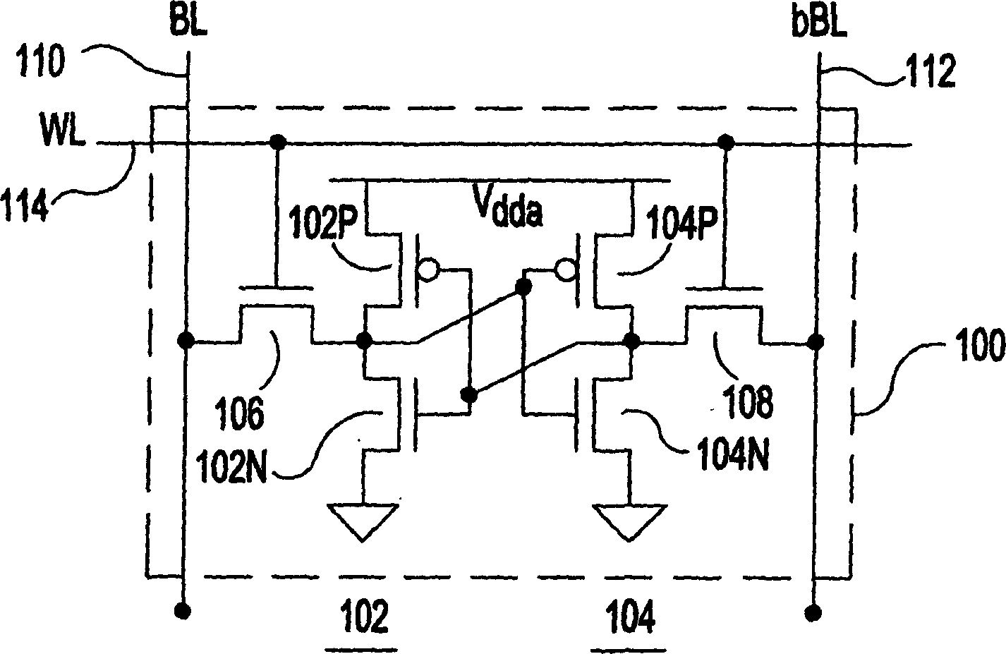
[0020] Referring now to the accompanying drawings, and more specifically, figure 1 A preferred embodiment of a six-transistor (6T) memory latch, e.g., static random access memory (SRAM) cell 100 in the well-known complementary insulated gate field-effect transistor (FET) technology known as CMOS is shown. Examples of embodiments. The technology has a stated design or design rule gate oxide thickness. Preferably, cell 100 is of what is known as partially depleted (PD) silicon-on-insulator (SOI) technology. By selectively providing increased threshold voltages (V T ) to reduce cell leakage, for example, by selectively thickening the gate oxide above the specified design gate oxide thickness, or forming the gate oxide with a high-k dielectric for these FETs. Thus, by using a suitable high-k gate dielectric or by increasing the thickness of the gate oxide or both, the threshold of the selected device is increased and thus the leakage of the device is reduced. Examples of high-...


PUM


Abstract

An integrated circuit that may include an array such as a static random access memory (SRAM) with high threshold device array devices and in selected other devices to reduce leakage. Devices with high threshold have a thicker gate oxide or a high k dielectric gate oxide that is selected based on threshold voltage (VT) variations with gate oxide dielectric type or gate oxide thickness for the particular technology, e.g., PD SOI CMOS. High threshold devices may be used in non-critical path margin identified. A thicker device threshold is selected for non-critical path FETs based on the non-critical path margin. Non-critical path delays are re-checked. FETs are formed with the selected thicker gate oxide for any non-critical paths passing the re-check and in array FETs with non-selected FETs being formed with normal gate oxide thickness.

Description

technical field [0001] The present invention relates to integrated circuit power consumption, and more particularly, to reducing the power consumption of static random access memory (SRAM). Background technique [0002] Advances in semiconductor technology and chip manufacturing have led to an increase in on-chip clock frequency, the number of transistors on a single chip, and die size, and a corresponding reduction in chip power supply voltage and chip feature size. In general, the power consumption of a given clocked cell increases linearly with its internal switching frequency if all other factors are fixed. Therefore, the power consumption of the chip increases despite the reduction of the chip supply voltage. At the chip and system level, cooling and packaging costs increase as chip power increases. For low-end systems where battery life is critical (for example, handheld, portable, and mobile systems), it is important to reduce net power consumption without reducing ...

Claims


Application Information

Patent Timeline
Patent Type & Authority Applications(China)
IPC IPC(8): G11C11/412H01L21/822H01L21/8238H01L21/8244H01L27/04H01L27/08H01L27/092H01L27/11
CPCG11C11/412
Inventor 庄青泰(音译)瑞杰弗·V·乔施麦克尔·G·罗森费尔德
Owner IBM CORP
Why Eureka
Try Eureka