

SOI CMOS device with reduced DIBL
a cmos device and dibl technology, applied in the field of cmos devices, can solve the problems of reducing the length of the channel of the cmos device, causing performance drawbacks, and causing performance limitations known as short channel effects
- Summary
- Abstract
- Description
- Claims
- Application Information
AI Technical Summary
Benefits of technology
Problems solved by technology
Method used
Image

Examples
Embodiment Construction
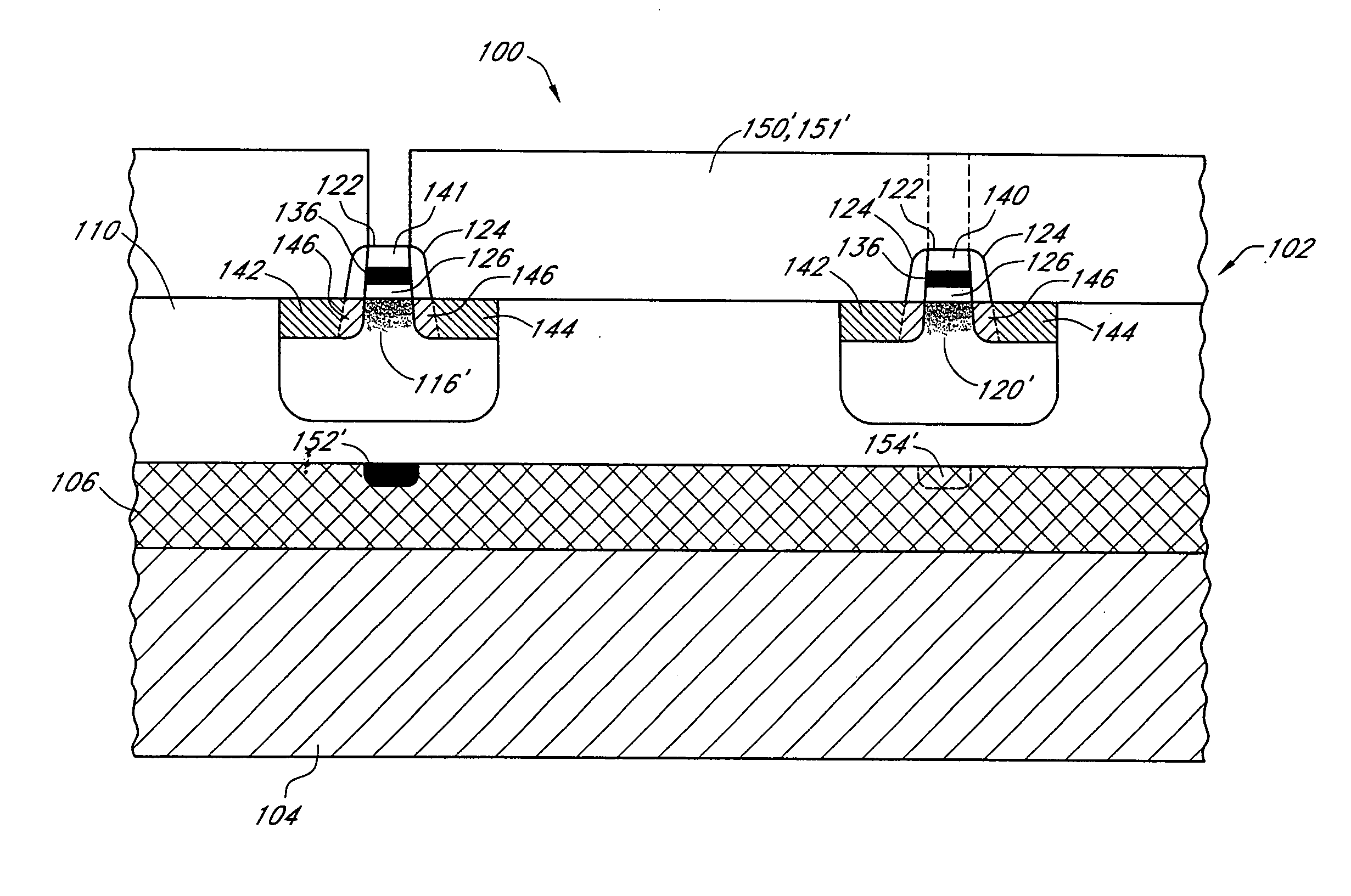
[0043] Reference will now be made to the drawings wherein like numerals refer to like structures or processes throughout. FIG. 4 is a section view of one embodiment of a method 100 of forming SOI CMOS with reduced DIBL 130 (FIG. 9) showing the starting SOI material, a Separation by IMplanted OXygen (SIMOX) wafer 102. The SIMOX wafer 102 is well known in the art and comprises a silicon substrate 104 in which a layer of the substrate 104 is converted to a buried silicon dioxide (BOX) 106 layer with a heavy oxygen implant and subsequent anneal. An epitaxial layer 110 of Si approximately 500 Å to 2500 Å thick is then grown on top of the BOX layer 106. The BOX layer 106 of the SIMOX wafer 102 provides electrical insulation between the active region provided by the epitaxial layer 110 and the bulk silicon of the substrate 104. Thus, active devices formed in the epitaxial layer 110 are electrically isolated from the semiconductive substrate 104. The SIMOX wafer 102 also provides physical s...
PUM
 Abstract
Description
Claims
Application Information