SOI CMOS compatible multiplanar capacitor

a multi-planar capacitor, cmos technology, applied in capacitors, semiconductor devices, diodes, etc., can solve the problems of low device density, severe performance degradation, and detrimental system malfunction

Active Publication Date: 2010-06-01
TWITTER INC
View PDF4 Cites 14 Cited by
  • Summary
  • Abstract
  • Description
  • Claims
  • Application Information

AI Technical Summary

Problems solved by technology

A small fluctuation in voltage or current of an electrical signal in such circuits may cause severe performance degradation, or even detrimental system malfunction.
However, a large surface area is occupied by these planar capacitors, resulting in a low device density and a large chip size, which decreases chip yield and may eventually increase cost if a large number of planar capacitors are employed in the integrated circuit.
Although deep trench capacitors have the advantage of providing high capacitance capacitors at a high areal density, this approach has several disadvantages that limit its application primarily to DRAM (Dynamic Random Access Memory) products.
First, forming deep trench capacitors requires a significant number of complicated and costly processing steps such as etching of deep trenches in a semiconductor substrate, forming buried capacitor plates, filling the deep trenches, etc.
Most of these processing steps are unique to deep trench technology, and thus, incompatible with conventional SOI CMOS processing sequence for logic devices such as a processor core.
Second, processing steps for manufacturing deep trenches increase total processing time for semiconductor chips, and consequently, increase the time-to-market of products employing deep trench capacitors.
Finally, this approach is costly because expensive equipment and heavy investment in research and development are required for the development deep trench related processes.

Method used


Image

  • SOI CMOS compatible multiplanar capacitor
  • SOI CMOS compatible multiplanar capacitor
  • SOI CMOS compatible multiplanar capacitor

Examples


Embodiment Construction

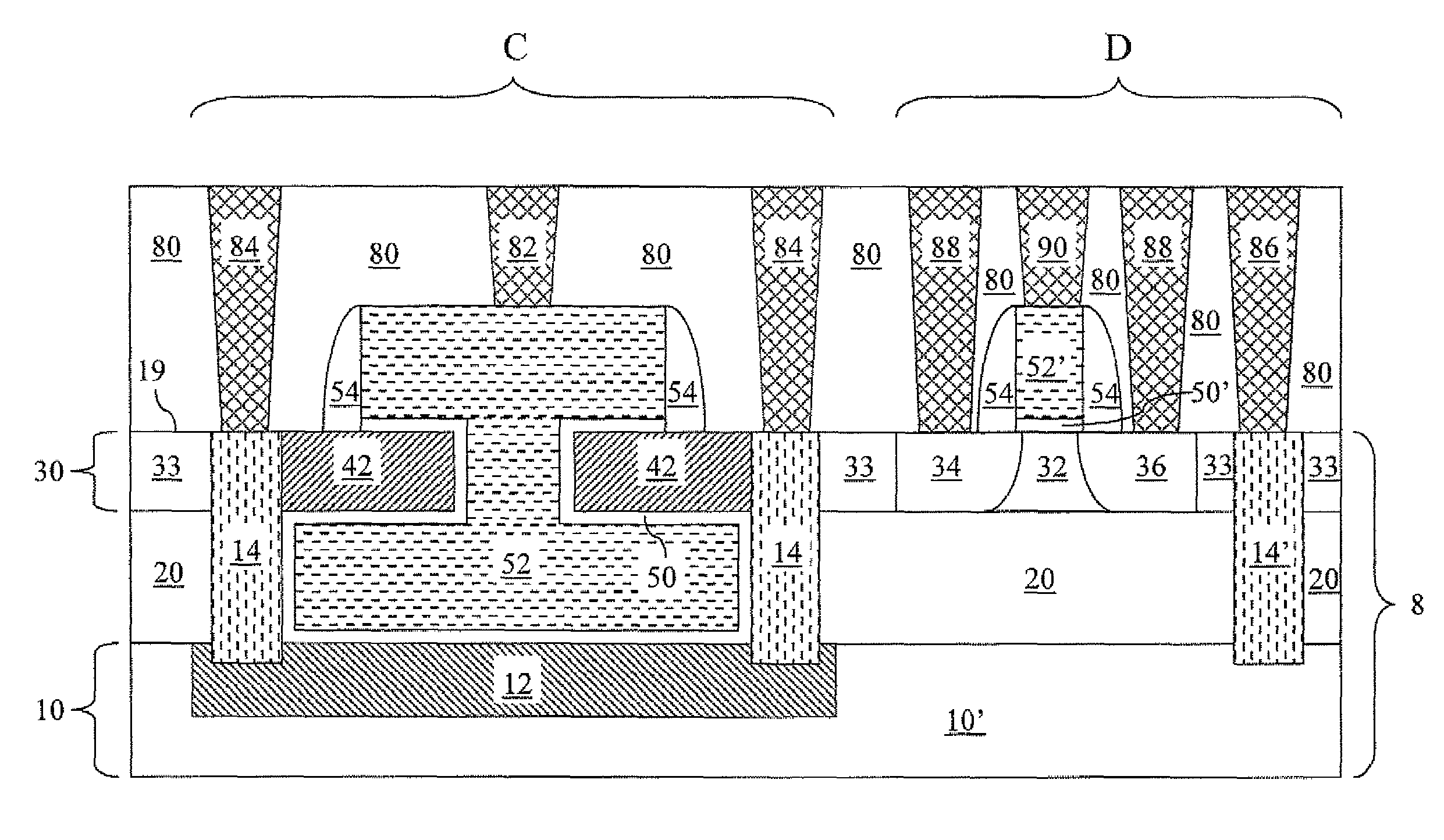
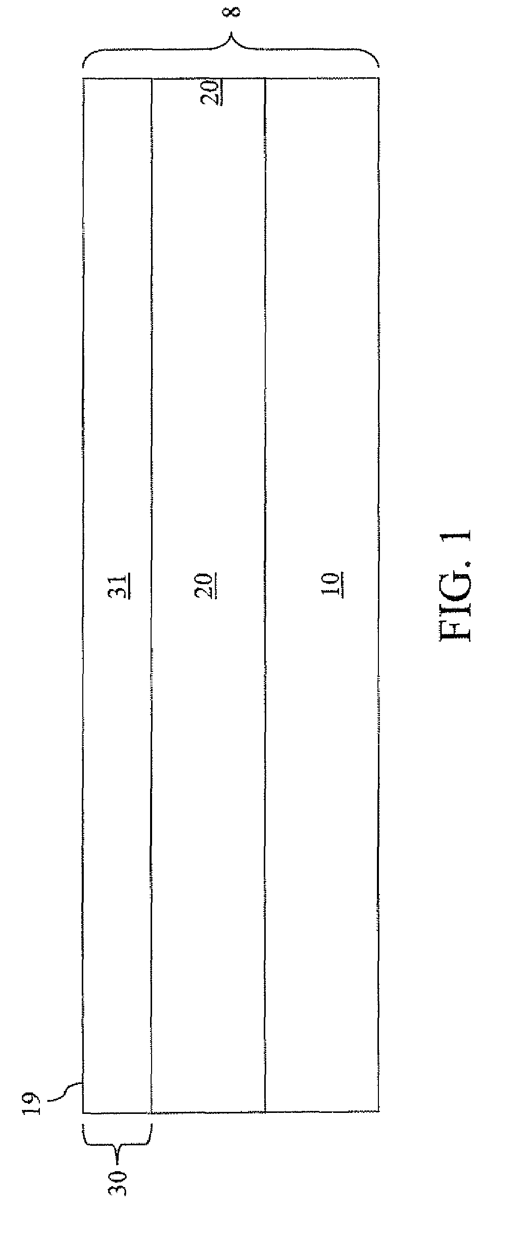
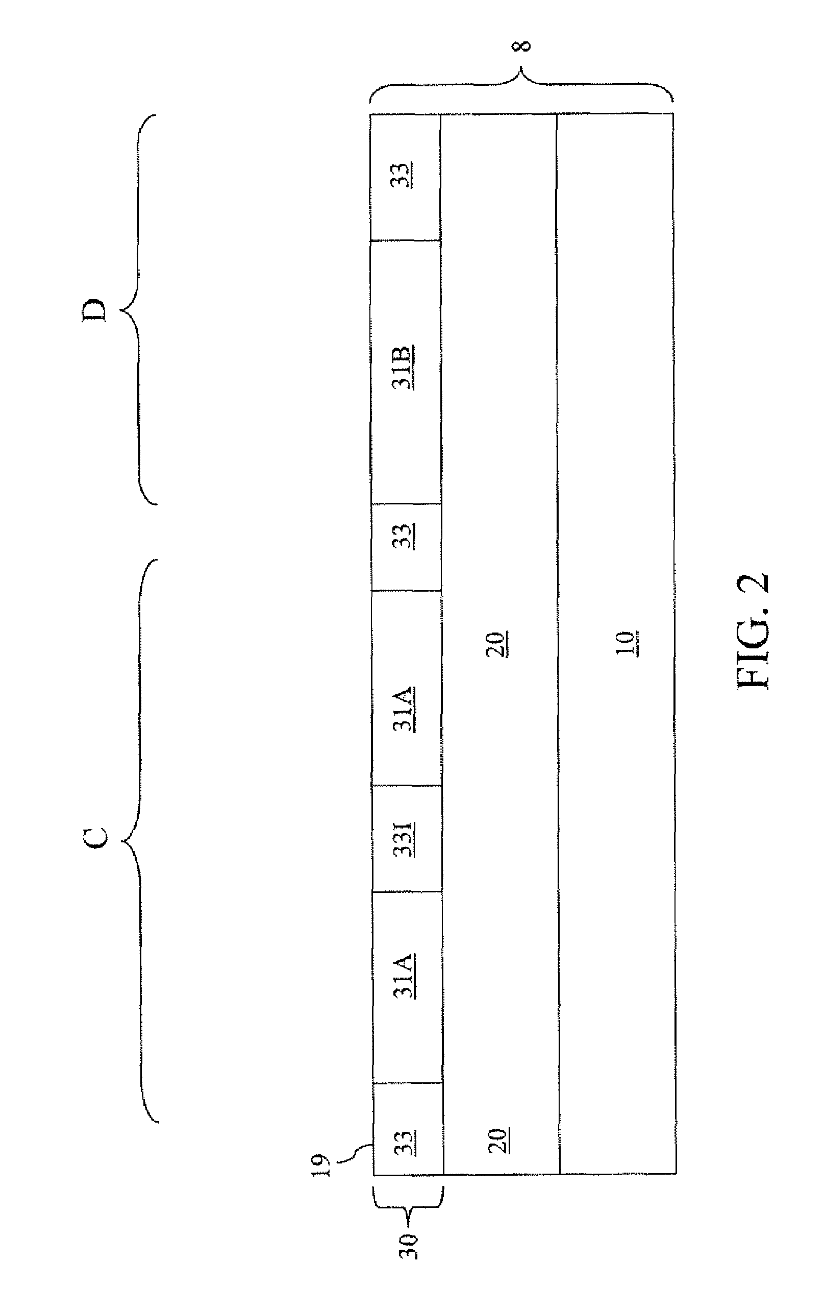
[0049]As stated above, the present invention relates to an SOI CMOS process compatible capacitor having multiplanar capacitor surfaces and methods of manufacturing the same, which are now described in detail with accompanying figures. It is noted that like and corresponding elements are referred to by like reference numerals.

[0050]Referring to FIG. 1, an exemplary semiconductor structure according to the present invention comprises a semiconductor-on-insulator (SOI) substrate 8 containing a handle substrate 10, a buried insulator layer 20, and a top semiconductor layer 30. The handle substrate 10 comprises a semiconductor material such as silicon. Preferably, the handle substrate 10 comprises a single crystalline semiconductor material. The handle substrate 10 may be undoped or have a p-type doping or an n-type doping. The conductivity of the doping of the handle substrate is herein referred to as a first conductivity type. The dopant concentration of the handle substrate 10 is from...


PUM


Abstract

An isolated shallow trench isolation portion is formed in a top semiconductor portion of a semiconductor-on-insulator substrate along with a shallow trench isolation structure. A trench in the shape of a ring is formed around a doped top semiconductor portion and filled with a conductive material such as doped polysilicon. The isolated shallow trench isolation portion and the portion of a buried insulator layer bounded by a ring of the conductive material are etched to form a cavity. A capacitor dielectric is formed on exposed semiconductor surfaces within the cavity and above the doped top semiconductor portion. A conductive material portion formed in the trench and above the doped top semiconductor portion constitutes an inner electrode of a capacitor, while the ring of the conductive material, the doped top semiconductor portion, and a portion of a handle substrate abutting the capacitor dielectric constitute a second electrode.

Description

FIELD OF THE INVENTION[0001]The present invention generally relates to semiconductor devices for integrated circuits, and particularly to a semiconductor-on-insulator (SOI) complementary metal oxide semiconductor (CMOS) process compatible capacitor having multiplanar capacitor surfaces and methods of manufacturing the same.BACKGROUND OF THE INVENTION[0002]Semiconductor-on-insulator (SOI) devices are increasingly employed in high performance integrated circuits for superior performance to bulk semiconductor devices. As the operating frequency of integrated circuits exceeds 1 gigahertz (GHz) with continued scaling of semiconductor devices, on-chip capacitors having a large capacitance are increasingly relied upon to maintain reliable functionality of high frequency integrated circuits. For example, decoupling capacitors are widely used in state-of-the art high frequency integrated circuits to suppress a voltage fluctuation in a power supply network during high speed switching operatio...

Claims


Application Information

Patent Timeline
Patent Type & Authority Patents(United States)
IPC IPC(8): H01L27/108
CPCH01L21/84H01L28/60H01L27/1203H01L27/10861H01L27/0629H10B12/038
Inventor CHENG, KANGGUOHSU, LOUIS CMANDELMAN, JACK A.TONTI, WILLIAM
Owner TWITTER INC
Why Eureka
Try Eureka