Coplaner waveguide and fabrication method thereof

a technology of waveguide and fabrication method, which is applied in the direction of optical elements, instruments, optics, etc., can solve the problems of small size high cost of monocrystalline compound semiconductor substrate, etc., to achieve the effect of cheap and easy fabrication of coplanar waveguides

Inactive Publication Date: 2010-03-11
OKI ELECTRIC IND CO LTD
View PDF3 Cites 8 Cited by
  • Summary
  • Abstract
  • Description
  • Claims
  • Application Information

AI Technical Summary

Benefits of technology

[0010]An object of the present invention is to provide a coplanar waveguide that can carry millimeter-wave signals on a monocrystalline silicon semiconductor substrate without the need for an insulating film having a thickness of 10 μm or more.
[0014]The signal line insulating film and ground conductor insulating film therefore need only be thick enough to insulate the signal line and ground conductors from the substrate and can be as thin as, for example, about 200 nm. As a result, the insulating film can be formed by conventional plasma CVD, making the coplanar waveguides inexpensive and easy to fabricate.

Problems solved by technology

Monocrystalline compound semiconductor substrates are, however, more expensive than monocrystalline silicon (Si) semiconductor substrates.
Because of the high cost and small size of monocrystalline compound semiconductor wafers, MMICs formed on monocrystalline compound semiconductor substrates are expensive.
Accordingly, forming insulating films of these materials 10 μm thick takes about 250 minutes and 720 minutes, respectively, which is impractical for commercial fabrication.
These additional processes differ from ordinary semiconductor processes and lead to increased fabrication cost.
Moreover, the film materials used by commercially available spin coaters do not readily yield films with thicknesses of 10 μm or more in one coating; two or more coating processes are required.
A baking process with a baking time of thirty minutes to one hour is necessary after each coating process, leading to an increase in fabrication time.
In addition, cracks may occur in the film in the second coating process.

Method used


Image

  • Coplaner waveguide and fabrication method thereof
  • Coplaner waveguide and fabrication method thereof
  • Coplaner waveguide and fabrication method thereof

Examples


Embodiment Construction

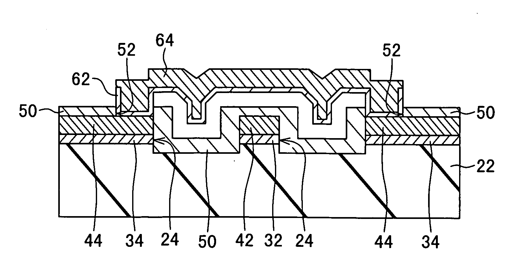
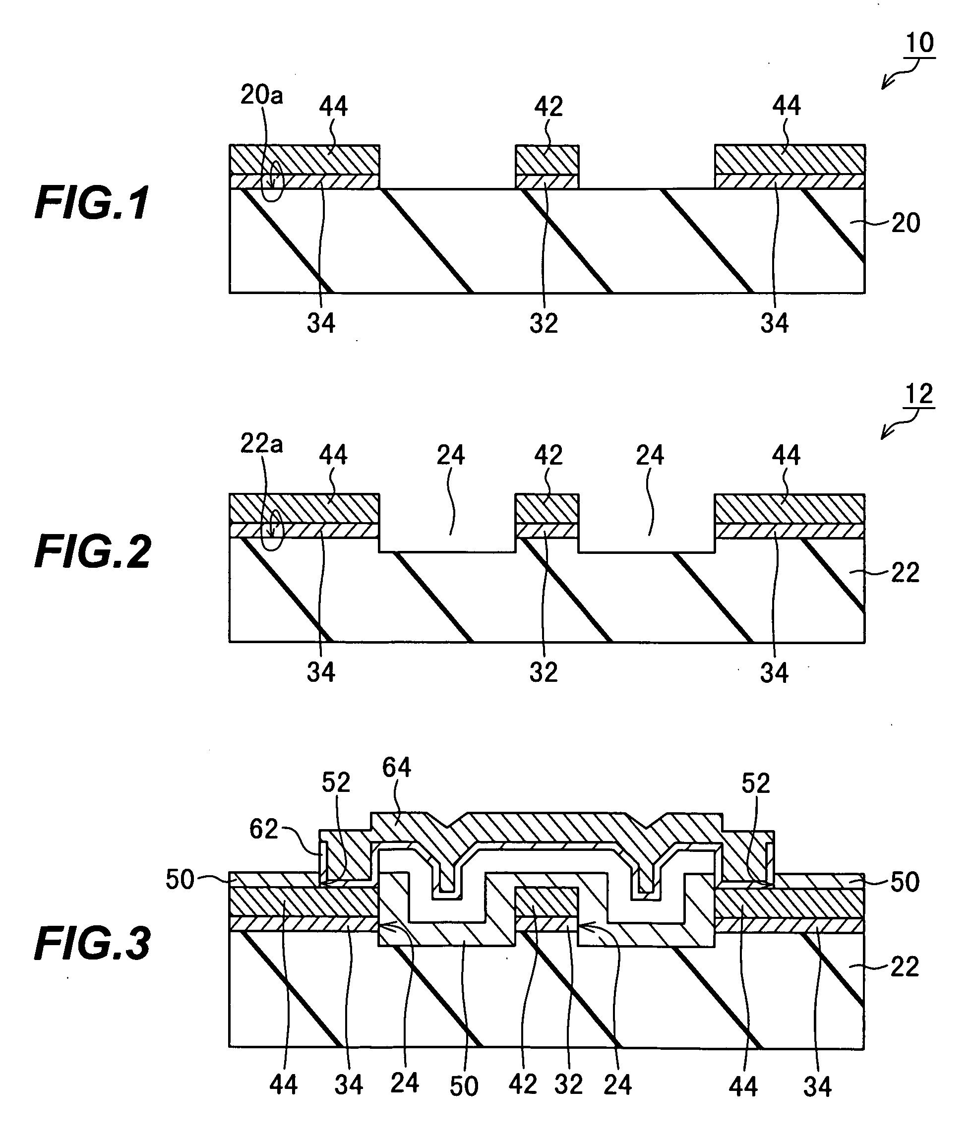
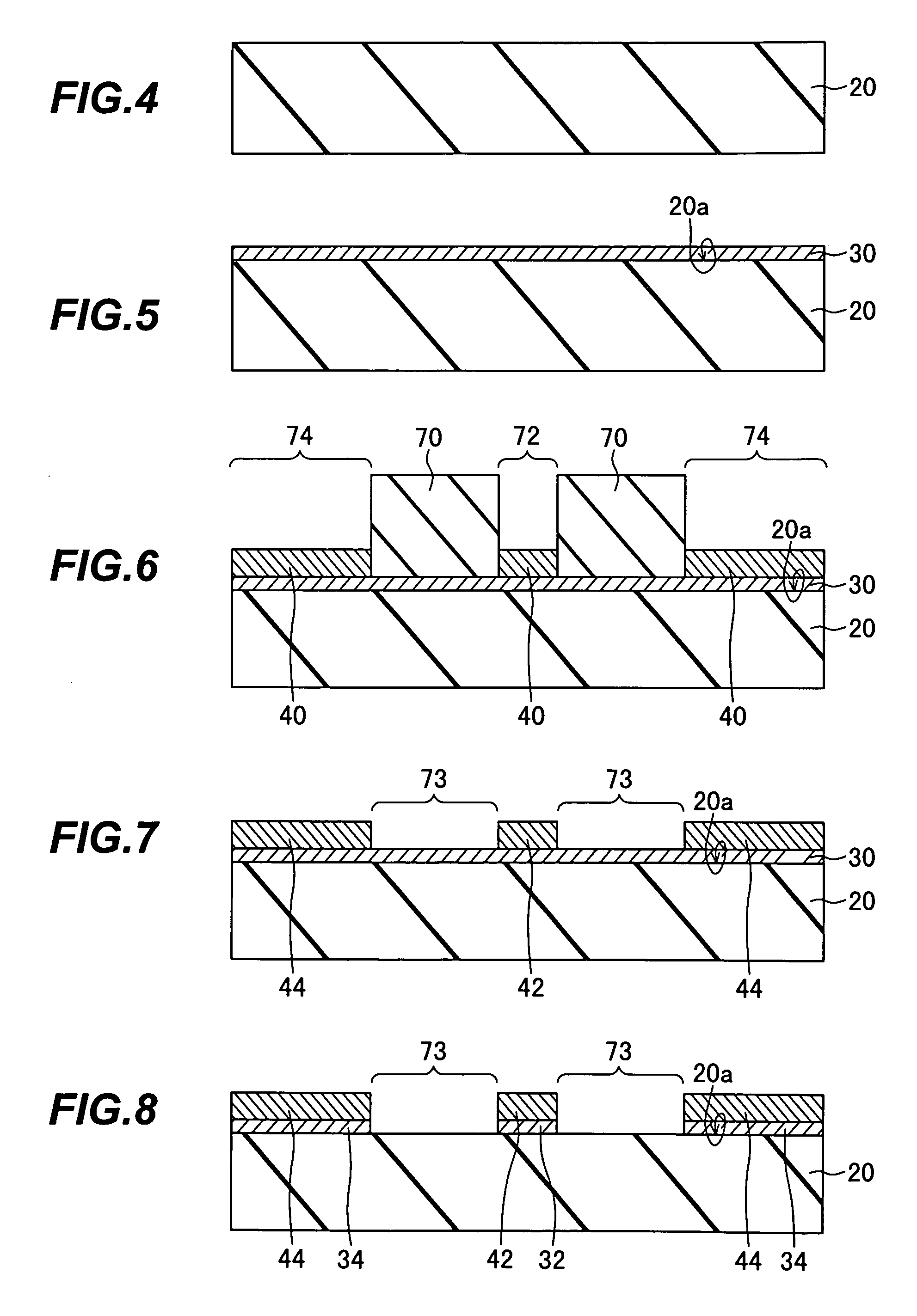
[0031]The invention will now be described in more detail with reference to the attached non-limiting drawings, in which like elements are indicated by like reference characters. Reference characters 20 and 22 will be used to denote flat and trenched substrates, respectively.

[0032]Referring to FIG. 1, a first coplanar waveguide 10 embodying the invention comprises a flat substrate 20, a signal line 42 formed on the substrate 20, and a pair of ground conductors 44 disposed on mutually opposite sides of the signal line 42. The signal line 42 and ground conductors 44 are insulated from the substrate 20 by insulating films formed on a major surface 20a of the substrate 20. The insulating film interposed between the substrate 20 and the signal line 42 is referred to as the signal line insulating film 32; the insulating film interposed between the substrate 20 and the ground conductors 44 is separate from the signal line insulating film 32 and is referred to as the ground conductor insulat...


PUM


Abstract

A coplanar waveguide includes a substrate, a signal line formed on the substrate, a pair of ground conductors formed on the substrate on mutually opposite sides of the signal line, a signal line insulating film disposed between the signal line and the substrate, and a ground conductor insulating film disposed between the pair of ground conductors and the substrate. No corresponding insulating film is present on the substrate between the signal line and the ground conductors. Even if a silicon substrate is used, the attenuation characteristics of the coplanar waveguide are comparable to the attenuation characteristics of coplanar waveguides formed on compound semiconductor substrates.

Description

BACKGROUND OF THE INVENTION[0001]1. Field of the Invention[0002]The present invention relates to a coplanar waveguide used for interconnecting integrated circuit elements operating in the millimeter-wave frequency band or connecting such circuit elements to package connectors, and to a coplanar waveguide fabrication method.[0003]2. Description of the Related Art[0004]In a monolithic microwave integrated circuit (MMIC) with active elements such as mixers and amplifiers and passive elements such as filters and capacitors, coplanar waveguides are used to interconnect the active and passive elements. Such coplanar waveguides generally comprise metal wiring patterns, and the substrate is generally a compound semiconductor substrate such as a gallium arsenide (GaAs) or indium phosphide (InP) substrate. One advantage of a compound semiconductor substrate is that its high electron mobility permits the formation of MMICs that can operate in the ten-gigahertz (10-GHz) band or higher. Another ...

Claims


Application Information

Patent Timeline
Patent Type & Authority Applications(United States)
IPC IPC(8): H01L23/52H01L21/768
CPCG02B6/136G02B2006/12061G02B2006/12097G02F2201/06G02F2202/10H01L23/66H01L2924/0002H01L2223/6627H01L2924/19033H01L2924/3011H01L2924/00
Inventor MAKITA, TAKESHITAMAI, ISAOHOSHI, SHINICHI
Owner OKI ELECTRIC IND CO LTD
Why Eureka
Try Eureka