
Semiconductor circuit

Inactive Publication Date: 2010-03-11
ADVANTEST CORP
View PDF2 Cites 4 Cited by
  • Summary
  • Abstract
  • Description
  • Claims
  • Application Information

AI Technical Summary

Benefits of technology

[0009]The “signal processing” means delay, amplification and filtering, etc., and the “characteristic value” refers to phase, amplitude and frequency, etc., of a signal. According to the embodiment, under the situation where a variation in a power supply voltage causes a variation in an amount of change provided to a characteristic value of an input signal by one of the signal processors, the variation in an amount of change in the characteristic value of the signal caused by the variation in a power supply voltage, which occurs in one of the signal processors, can be cancelled by the other of the signal processors. As a result, a variation in an amount of change provided to a characteristic value of an input signal by the whole semiconductor circuit, can be suppressed.
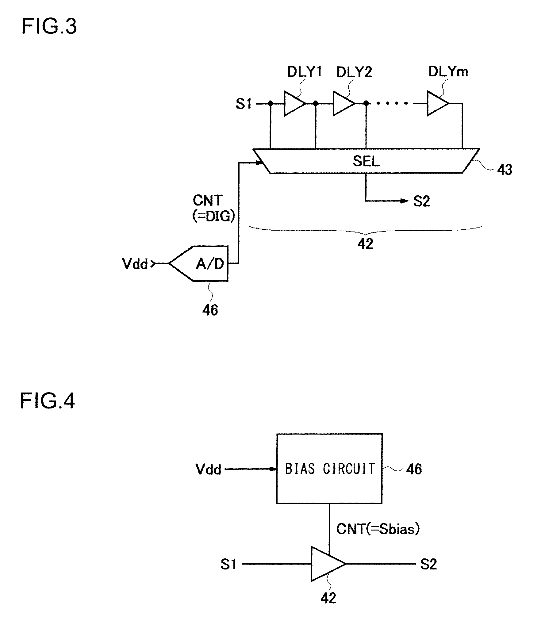
[0012]The first and second signal processors may be delay circuits. In this case, a delay amount provided to an input signal by the whole semiconductor circuit can be stabilized, allowing a signal with less jitter to be generated.
[0015]Another embodiment of the present invention is a test apparatus. This test apparatus comprises the aforementioned semiconductor circuit to provide a delay to an inputted clock. By using the semiconductor circuit, jitter in a delay amount provided to the clock can be suppressed, allowing the test accuracy to be enhanced.

Problems solved by technology

That is, there are problems that, in the case of a delay circuit, jitter is superimposed on a delay amount; and in the case of an amplifier, a ripple is superimposed on an amplitude of a signal.

Method used


Image

  • Semiconductor circuit
  • Semiconductor circuit
  • Semiconductor circuit

Examples


Embodiment Construction

[0026]The invention will now be described based on preferred embodiments which do not intend to limit the scope of the present invention but exemplify the invention. All of the features and the combinations thereof described in the embodiment are not necessarily essential to the invention.

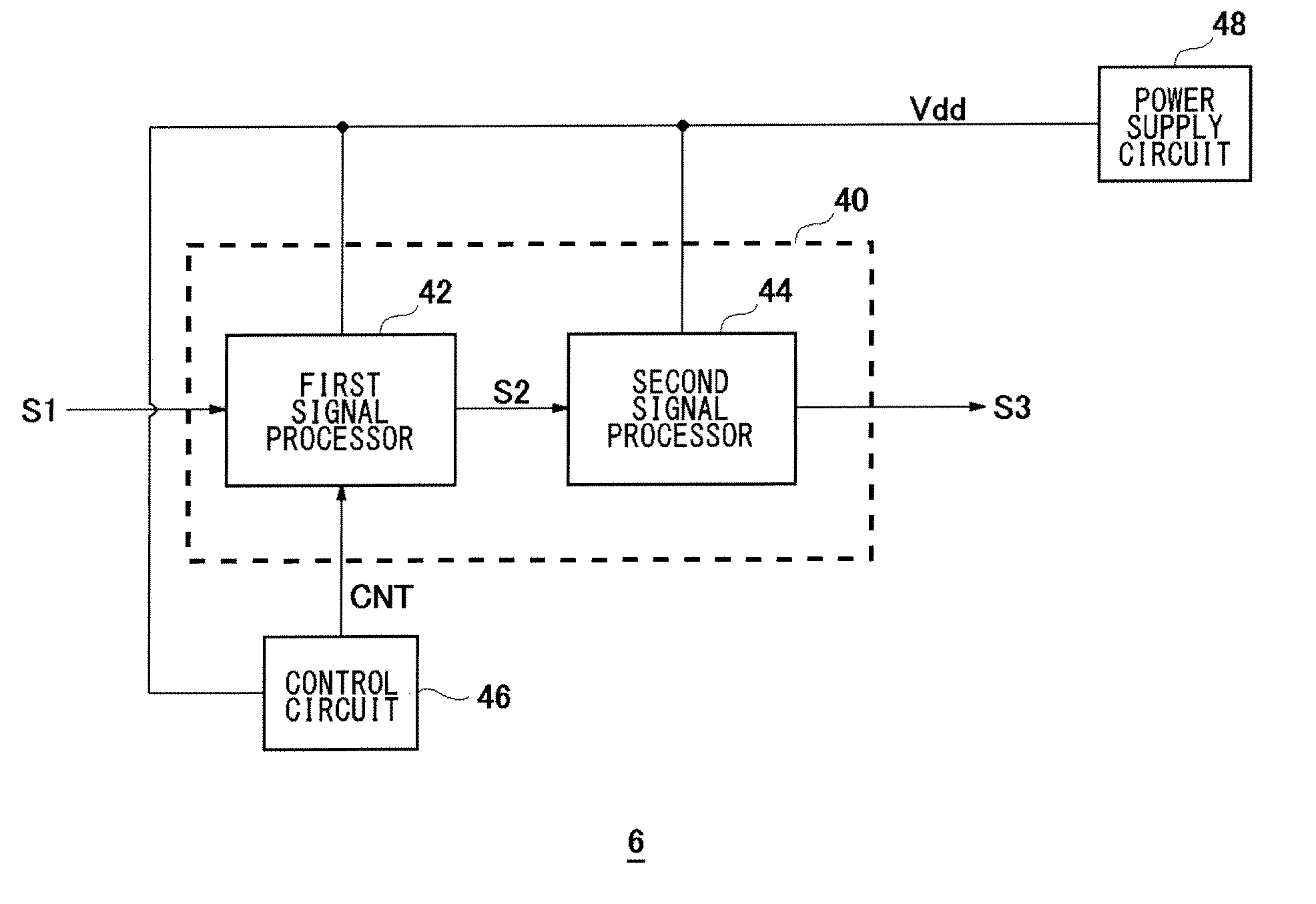
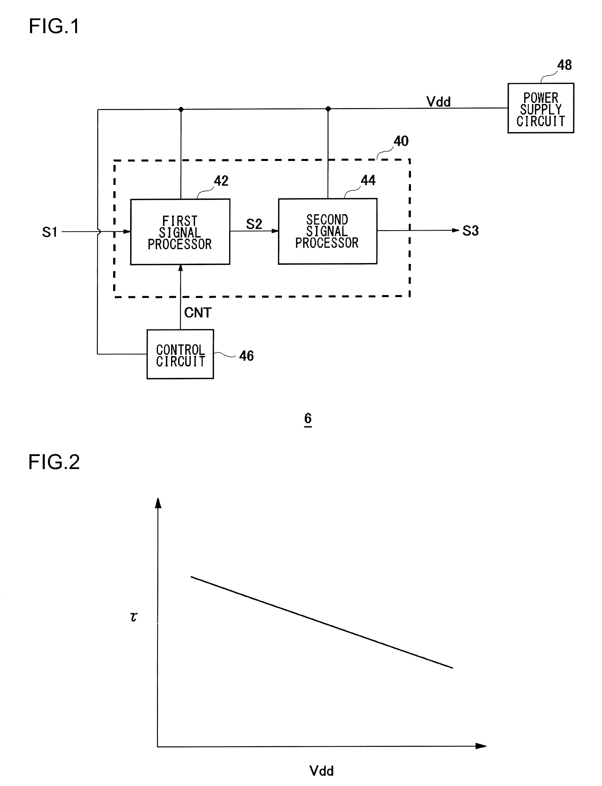
[0027]FIG. 1 is a block diagram illustrating the configuration of the semiconductor circuit 6 according to the embodiment of the present invention. The semiconductor circuit 6 performs as a whole predetermined signal processing on an input signal S1 and generates an output signal S3. A content of the signal processing is not limited, but at least one of characteristic values of the input signal S1 is provided with a change. For example, if the signal processing is delay processing, the phase (timing at the edge) of the input signal S1, a characteristic value of the signal, is provided with a change. Besides, if the signal processing is amplification processing, the amplitude of the input signal S1,...


PUM


Abstract

A first signal processor performs predetermined signal processing on an input signal to provide a change to at least one of the characteristic values thereof. A second signal processor is provided in the subsequent stage of the first signal processor and performs predetermined signal processing on an output signal from the first signal processor to provide a change to a characteristic value thereof. An amount of change provided to the characteristic value of the signal by the second signal processor is dependent on a power supply voltage. An amount of change provided to the characteristic value of the signal by the first signal processor is configured to be adjustable. A control circuit monitors a power supply voltage supplied to the second signal processor and adjusts in accordance with the power supply voltage the amount of change provided to the characteristic value of the signal by the first signal processor.

Description

CLAIM OF PRIORITY TO RELATED APPLICATION[0001]The present application is claiming priority of Japanese Patent Application No. 2008-078013, filed on Mar. 25, 2008, the content of which is incorporated herein by reference.BACKGROUND OF THE INVENTION[0002]1. Field of the Invention[0003]The present invention relates to a semiconductor circuit that performs certain signal processing on an input signal.[0004]2. Description of the Related Art[0005]Signal processing circuits, which perform certain signal processing on an input signal to provide a change to a characteristic value of the signal, for example, phase, amplitude and frequency characteristic, and output the signal thus changed, are widely used for various semiconductor circuits (hereinafter, referred to as ICs). Examples of such signal processing circuits include a delay circuit, amplifier, filter, and the like.[0006]An amount of change provided to a characteristic value of a signal by the above signal processing circuit is someti...

Claims


Application Information

Patent Timeline
IPC IPC(8): H03K5/13H03K5/01H03F1/30H03K5/131H03K5/14H03K17/16
CPCH03F1/30H03F2200/459H03K2005/00234H03K2005/0013H03K2005/00156H03K5/13
Inventor KOJIMA, SHOJIOKAYASU, TOSHIYUKI
Owner ADVANTEST CORP
Learn More