IC socket

Active Publication Date: 2018-08-23
YAMAICHI ELECTRONICS
View PDF1 Cites 11 Cited by
  • Summary
  • Abstract
  • Description
  • Claims
  • Application Information

AI Technical Summary

Benefits of technology

[0016]The IC socket according to the present invention comprises: the upper housing made of the electrically conductive material and including the plurality of holes configured to individually accommodate the contact terminals at given clearance; the base member made of the electrically conductive material, provided on the one end surface of the upper housing, including the holes each configured to allow passage of the first plunger of each of the contact terminals while retaining the predetermined clearance, and configured to support the first plunger inside each hole through the collar made of the dielectric body; and the lower housing made of the electrically conductive material, provided on the other end su

Problems solved by technology

However, the clearance may cause a deviation of the axis of the upper plunger and the lower plunger from the center of the supporting hole in the dielectric body, which is likely to result in the deviation of the impedance without achieving prescribed concentricity.
Moreover, there is al

Method used


Image

  • IC socket
  • IC socket
  • IC socket

Examples


Example

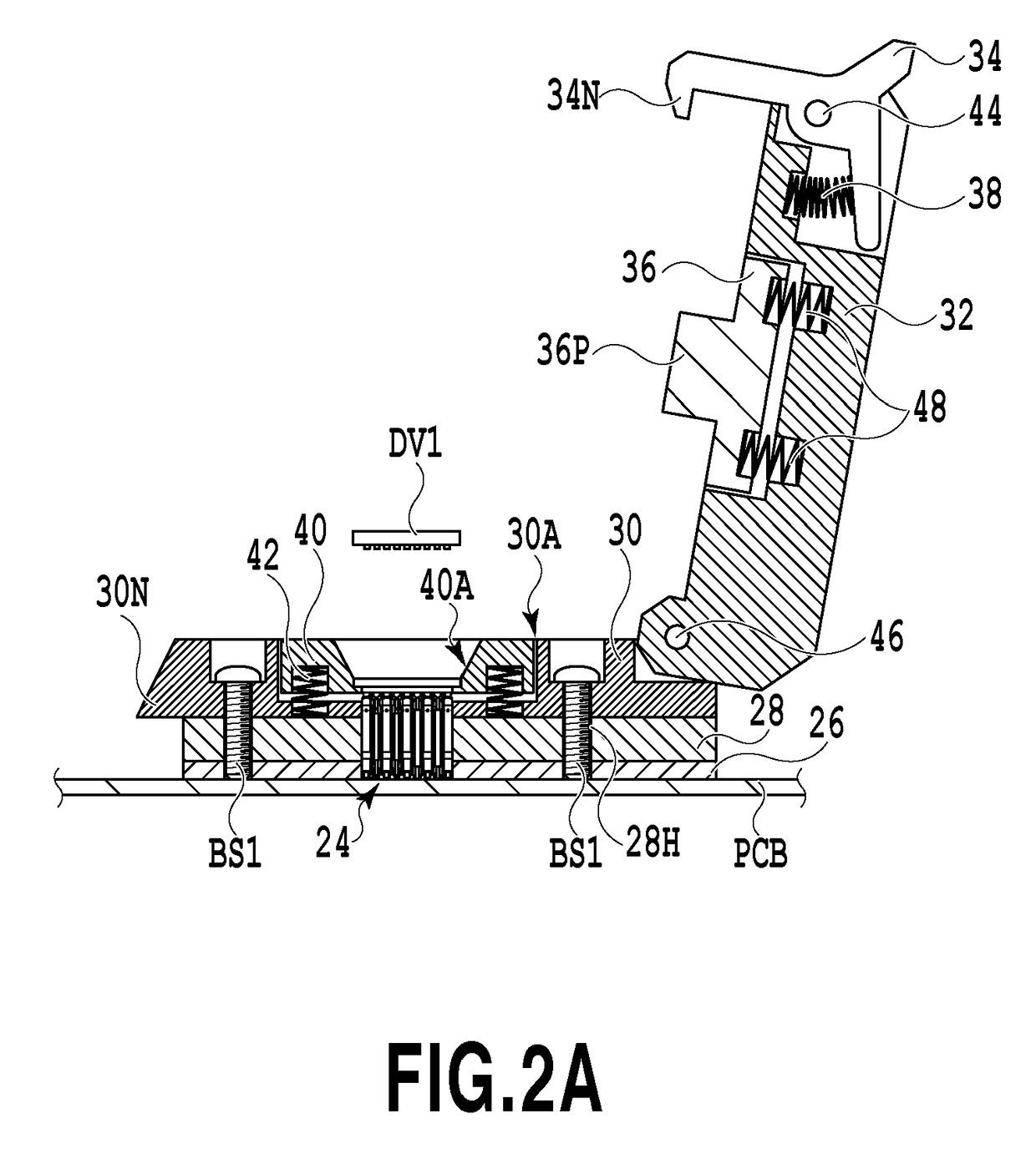
[0059]FIG. 2A schematically shows a configuration of a first embodiment of an IC socket according to the present invention.

[0060]In FIG. 2A, a plurality of IC sockets are disposed on a printed wiring board PCB serving as a test board, for example. Note that FIG. 2A representatively illustrates one IC socket on the printed wiring board PCB.

[0061]The printed wiring board PCB is made of glass epoxy resin, for example, and has an electrode group (not shown) which is provided with a plurality of electrode pads that are formed in a matrix corresponding to a layout of contact terminals to be described later, and is located at a substantially central part on one of surface portions. Through-holes into which machine screws to be described later are inserted are formed at four positions around the electrode group.

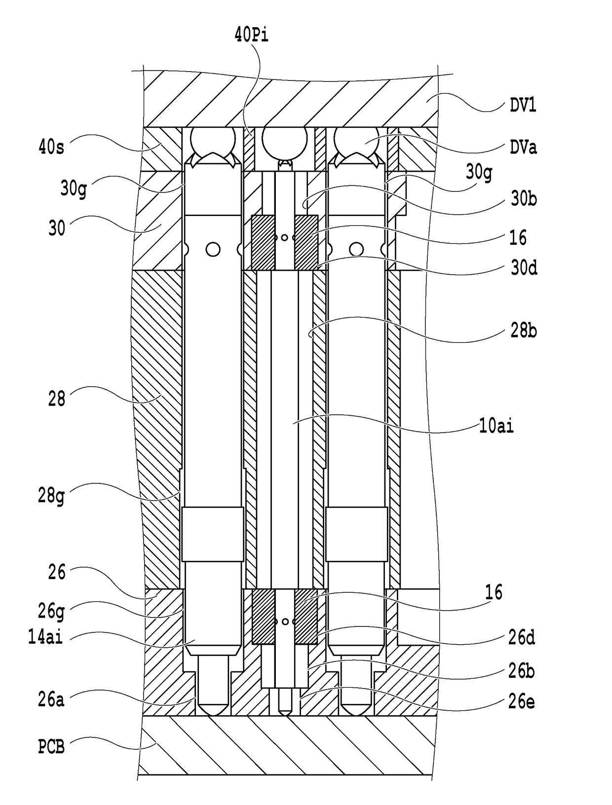
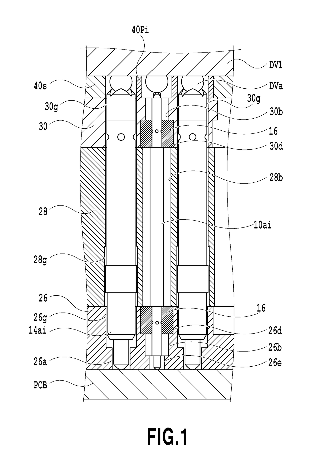
[0062]For example, the IC socket is provided with a pressing mechanism unit of a clam shell type, an upper housing 28, a lower housing 26, and a contact terminal group 24 to be provi...

Example

[0133]FIG. 14A schematically shows a configuration of a second embodiment of an IC socket according to the present invention.

[0134]In FIG. 14A, a plurality of IC sockets are disposed on the printed wiring board PCB serving as the test board, for example. Note that FIG. 14A representatively illustrates one IC socket on the printed wiring board PCB. Here, constituents in FIGS. 14A, 14B, and 15 which are the same as the constituents in FIGS. 2A, 2B, and 2C will be denoted by the same reference signs and overlapping explanations thereof will be omitted.

[0135]For example, the IC socket includes the pressing mechanism unit of a clam shell type, the upper housing 28, the lower housing 26, and a contact terminal group to be provided inside the upper housing 28 and the lower housing 26.

[0136]The pressing mechanism unit includes the base member 30 placed on the upper end surface of the upper housing 28 through a sheet 50, and the lid member 32 rotationally movably supported by the end portion...


PUM


Abstract

When each signal line contact terminal (10ai) is installed in a base member (30), an upper housing (28), and a lower housing (26), the upper housing (28) is installed together in such a way as to be sandwiched between the base member (30) and the lower housing (26). Here, collars (16) are fitted on outer peripheral portions of a first extending portion (52A) and a second extending portion (52C) of the signal line contact terminal (10ai), respectively. Moreover, air layers are formed between an outer peripheral portion of a drum portion (52B) of the signal line contact terminal (10ai) and an inner peripheral surface forming a hole (28b), between an outer peripheral portion of the first extending portion (52A) and an inner peripheral surface forming a hole (30b), between an outer peripheral portion of the second extending portion (52C) and an inner peripheral surface forming a hole (26b), and between an outer peripheral portion of a plunger (56) and an inner peripheral surface forming a hole (26e).

Description

TECHNICAL FIELD[0001]The present invention relates to an IC socket.BACKGROUND ART[0002]A semiconductor device serving as an electronic device to be mounted on an electronic equipment or the like is generally subjected to a test for eliminating potential defects therein by using an Integrated Circuit socket (IC socket) at a stage before the semiconductor device is mounted. As shown in PATENT DOCUMENT 1, for example, such an IC socket is provided on a printed wiring board (a test board or a mounting board).[0003]In the case where a semiconductor device socket is provided in a transmission line that transmits an RF (radio frequency) signal in a relatively high frequency band such as 1 GHz or above, there has been known a technique for enhancing a transmission performance of a signal in a relatively high frequency band by subjecting an IC socket to impedance matching in order to enhance the transmission performance of the signal in the relative high frequency band, and decreasing induct...

Claims


Application Information

Patent Timeline
IPC IPC(8): G01R31/26H01R33/76G01R1/04G01R1/067
CPCG01R31/26H01R33/76G01R1/0433G01R1/06722G01R1/045G01R1/0466H01R13/2421H01R24/50H05K7/1007H05K7/1061
Inventor NAKAMURA, YUJIIWATA, MASASHI
Owner YAMAICHI ELECTRONICS
Why Eureka
Try Eureka