

Array substrate and defect-detecting method thereof
a defect detection and array substrate technology, applied in the field of liquid crystal display, can solve the problems of human error for visual inspection, reduce production speed, form display defects in liquid crystal panels, etc., and achieve the effect of accurately and quickly locating the defect line on the array substra
- Summary
- Abstract
- Description
- Claims
- Application Information
AI Technical Summary
Benefits of technology
Problems solved by technology
Method used
Image

Examples
first embodiment
The First Embodiment
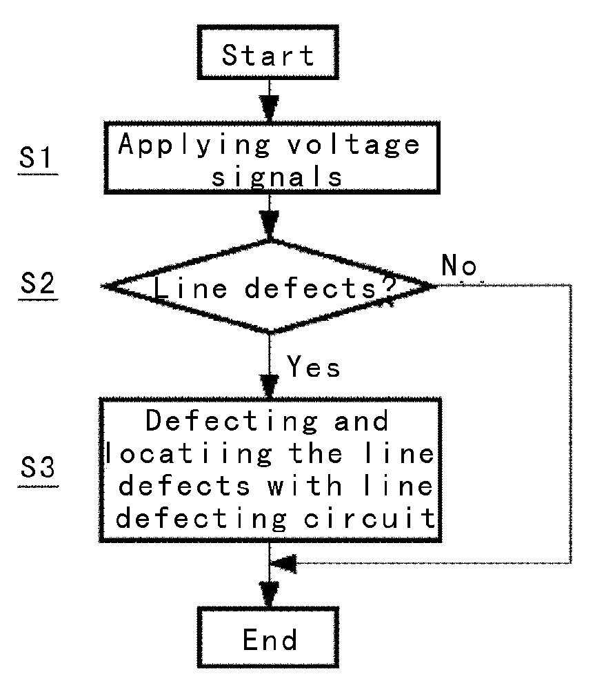
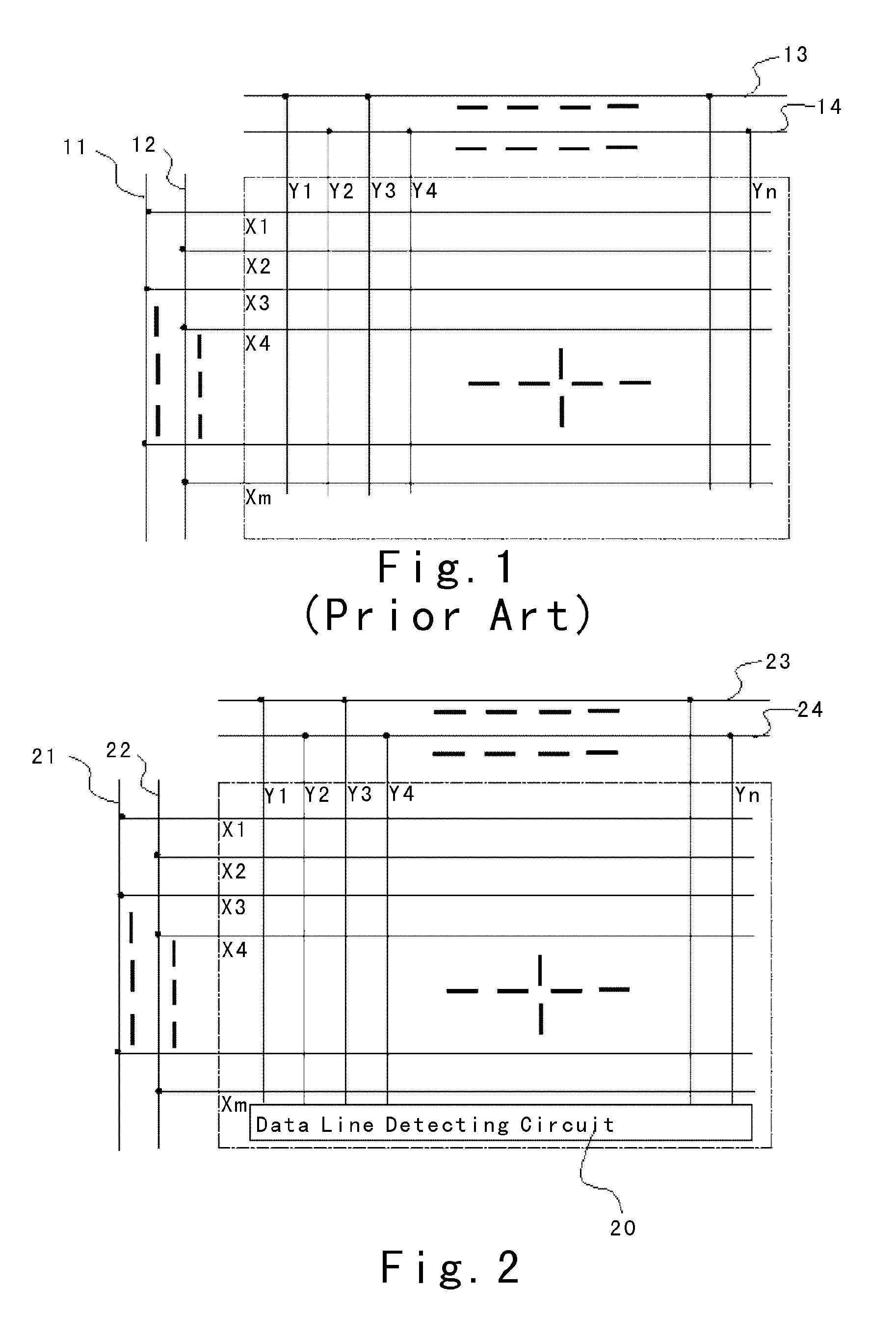
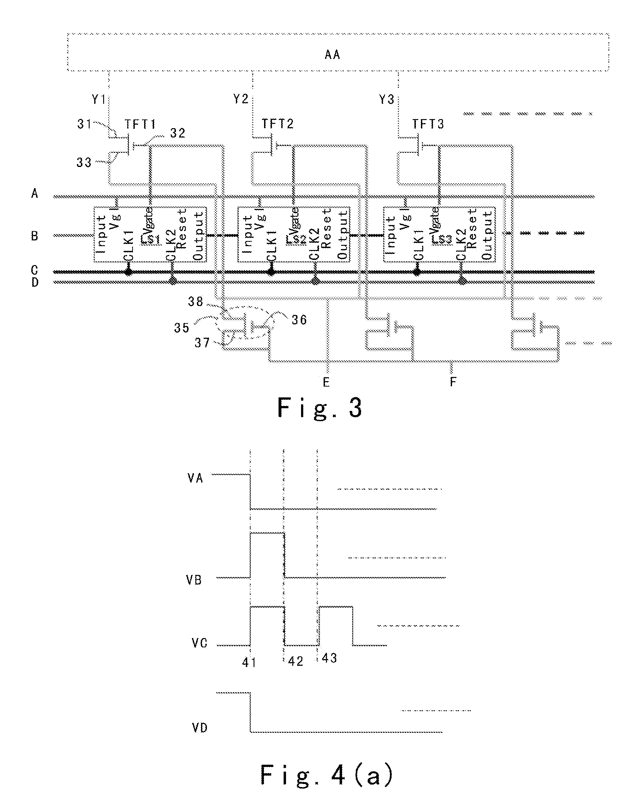
[0020]The first embodiment of the invention will be described first with reference to FIGS. 2 to 6B. FIG. 2 is a schematic diagram illustrating an array substrate that is provided with a data line detecting circuit in accordance with a first embodiment of the invention. The array substrate has m rows and n columns, and comprises at the periphery thereof (i.e., in an empty area other than the array substrate of a mother glass substrate) the following: a first gate shorting bar 21 electrically connecting with the odd gate lines (X1, X3, . . . , Xm-1), a second gate shorting bar 22 electrically connecting with the even gate lines (X2, X4, . . . , Xm), a first data shorting bar 23 electrically connecting with the odd data lines (Y1, Y3, . . . , Yn-1), and a second data shorting bar 24 electrically connecting with the even data lines (Y2, Y4, . . . , Yn). The array substrate of the first embodiment further comprises a data line detecting circuit 20 set in the non-disp...
second embodiment
The Second Embodiment
[0032]The above description is directed to an array substrate for detecting and locating line defects of data lines and the method thereof. For the gate lines, a similar gate line detecting circuit may be used to perform processing. Referring to FIG. 7, which is a schematic diagram illustrating an array substrate that is provided with a gate line detecting circuit 70 in accordance with the second embodiment of the invention. As shown in FIG. 7, the gate line detecting circuit 70 is set in the non-display area of the right part of the array substrate. The gate line detecting circuit 70 as shown in FIG. 7 can receive the voltage signals transmitted by the gate lines so as to detect and locate the line defects of the gate lines. The gate line detecting circuit 70 may have the same configuration as the data line detecting circuit of the first embodiment except connecting to m gate lines. In addition, the gate line detecting method that is performed with the gate lin...
third embodiment
The Third Embodiment
[0033]Other than providing only a data line detecting circuit or a gate line detecting circuit, a data line detecting circuit and a gate line detecting circuit may be provided simultaneously to detect the defects of the data lines and gate lines. FIG. 8 is a schematic diagram illustrating an array substrate that is provided with a data line detecting circuit and a gate line detecting circuit in accordance with the third embodiment of the invention. As shown in FIG. 8, a data line detecting circuit 80 and a gate line detecting circuit 90 are set in the non-display areas of the lower and right parts of the array substrate respectively. The data line detecting circuit 80 as shown in FIG. 8 can receive the voltage signals transmitted by the data lines so as to detect and locate the line defects of the data lines. The gate line detecting circuit 90 can receive the voltage signals transmitted by the gate lines so as to detect and locate the line defects of the gate lin...
PUM
 Abstract
Description
Claims
Application Information