Top exposed clip with window array

a technology of window array and exposed clip, which is applied in the direction of semiconductor devices, semiconductor/solid-state device details, electrical apparatus, etc., can solve the problems of not being able to meet the pinout of standard lead frame, the die package requires flip-chip process, etc., to reduce the spreading resistance, and add mechanical strength to the package

a technology of window array and exposed clip, which is applied in the direction of semiconductor devices, semiconductor/solid-state device details, electrical apparatus, etc., can solve the problems of not being able to meet the pinout of standard lead frame, the die package requires flip-chip process, etc., to reduce the spreading resistance, and add mechanical strength to the package

US20100072585A1Active Publication Date: 2010-03-25ALPHA & OMEGA SEMICON INC

Image

  • Top exposed clip with window array
  • Top exposed clip with window array
  • Top exposed clip with window array

Examples


Embodiment Construction

[0021]Although the following detailed description contains many specific details for the purposes of illustration, anyone of ordinary skill in the art will appreciate that many variations and alterations to the following details are within the scope of the invention. Accordingly, the examples of embodiments of the invention described below are set forth without any loss of generality to, and without imposing limitations upon, the claimed invention.

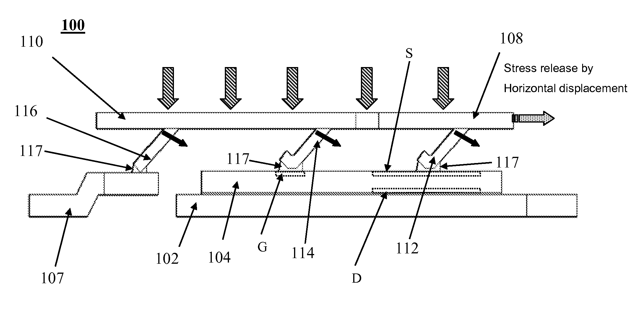
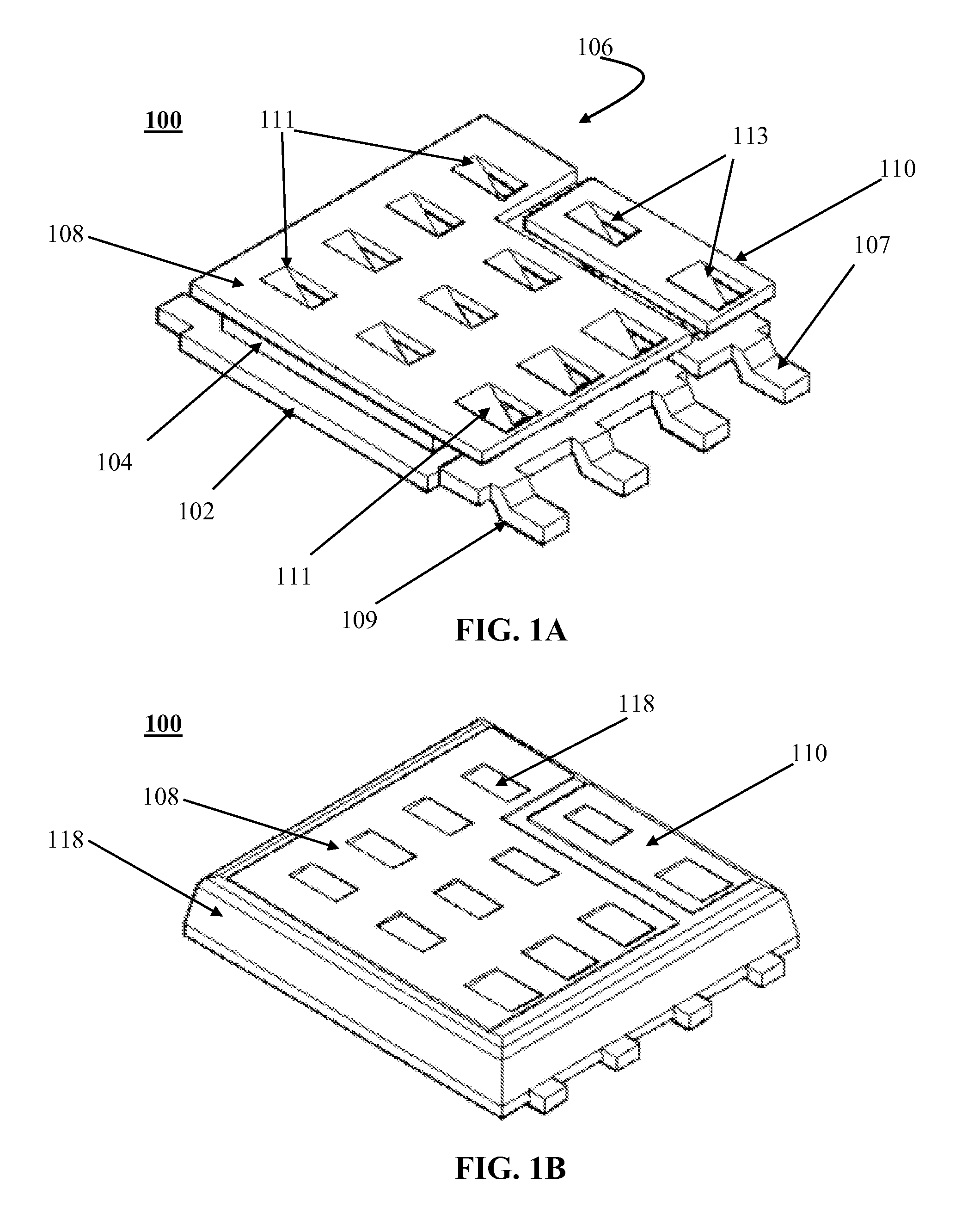
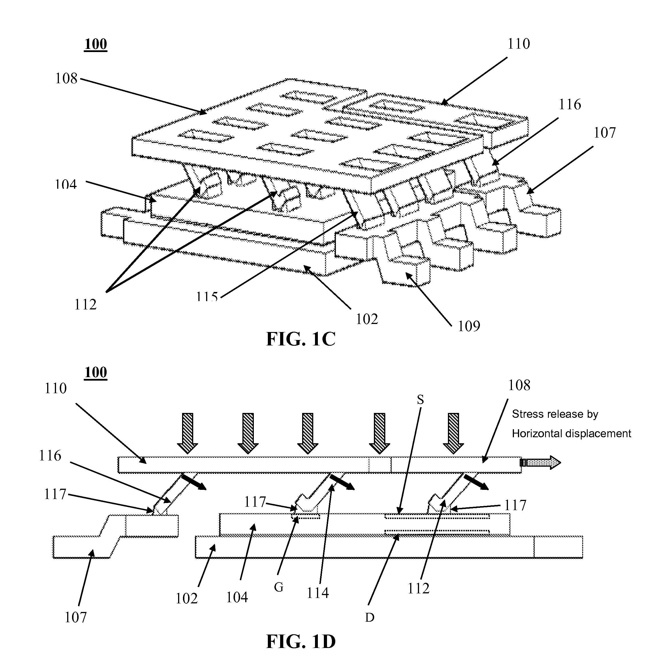
[0022]FIGS. 1A-1D depict a semiconductor device package 100 according to an embodiment of the present invention. In the example shown in FIGS. 1A and 1C, the device package 100 includes a fused lead frame 102 and a semiconductor device 104 having contact regions on top and bottom surfaces. The contact regions are formed from exposed regions of metal or other electrically conductive material that are in electrical contact with corresponding semiconductor device structures within the semiconductor device 104. By way of example, but not by wa...


PUM


Abstract

A clip for a semiconductor device package may include a metal sheet including an array of windows and one or more conductive fingers. Each of the conductive fingers has a first end and a second end. The first end is electrically connected to the metal sheet at one of the windows. Each of the conductive fingers is adapted to provide electrical connection to a top semiconductor region of a semiconductor device or a lead frame at the second end.

Description

FIELD OF THE INVENTION[0001]This invention generally relates to semiconductor die packages and more particularly to the use of a source clip in a die package to provide electrical contact in a way that lowers spreading resistance and enhances heat dissipation.BACKGROUND OF THE INVENTION[0002]In semiconductor device packaging, a metallic clip is often used to provide electrical connections between a semiconductor die and a lead frame to which the die is mounted. Most current clips are non-exposed clips. Some clips may be exposed for better heat dissipation, but have limitations. For example, U.S. Pat. No. 6,624,522 discloses a metal oxide semiconductor (MOS) gated device wafer having a source side covered with a passivation layer, preferably a photosensitive liquid epoxy, or a silicon nitride layer, or the like. The wafer is coated by a spinning, screening, or otherwise depositing the liquid epoxy onto the wafer surface. The material is then dried and the coated wafer is exposed usin...

Claims


Application Information

Patent Timeline
25 Mar 2010
Publication
US20100072585A1
IPC
H01L23/495; H01L21/56
CPC
H01L21/565; H01L2924/1305; H01L23/49524; H01L23/49551; H01L23/49562; H01L24/40; H01L24/72; H01L2924/01013
Inventors
SHI, LEI; LIANG, ZHAO