Solar cell and method of manufacturing the same

a solar cell and manufacturing method technology, applied in the direction of semiconductor/solid-state device manufacturing, electrical equipment, semiconductor devices, etc., can solve the problems of affecting the performance of the material, so as to achieve a wide range of lines and high carrier-collection efficiency.

Active Publication Date: 2010-04-01
PANASONIC INTELLECTUAL PROPERTY MANAGEMENT CO LTD
View PDF11 Cites 12 Cited by
  • Summary
  • Abstract
  • Description
  • Claims
  • Application Information

AI Technical Summary

Benefits of technology

[0011]According to the first aspect of the invention, the first-conductivity-type semiconductor layer is formed as plural island-shaped sections arranged side by side in the predetermined direction. Even though a metal mask is used for forming the first-conductivity-type semiconductor layer, the first-conductivity-type semiconductor layer can have a thinner line width by using a metal mask. Further, according to the first aspect, since the conductive layer is formed by a printing method, the thinner lined conductive layer can be formed to bridge adjacent two of the plural island-shaped sections. A solar cell having high carrier-collection efficiency can thereby be manufactured.

Problems solved by technology

However, the metal mask with such a structure has a lower strength, and thus tends to have some portions broken or bent (raised).
This may cause a problem of damaging the surface of the semiconductor substrate or misaligning the pattern.
For this reason, there is a limitation to a microscopic formation of n type semiconductor regions and p type semiconductor regions by means of metal masks.

Method used


Image

  • Solar cell and method of manufacturing the same
  • Solar cell and method of manufacturing the same
  • Solar cell and method of manufacturing the same

Examples


Embodiment Construction

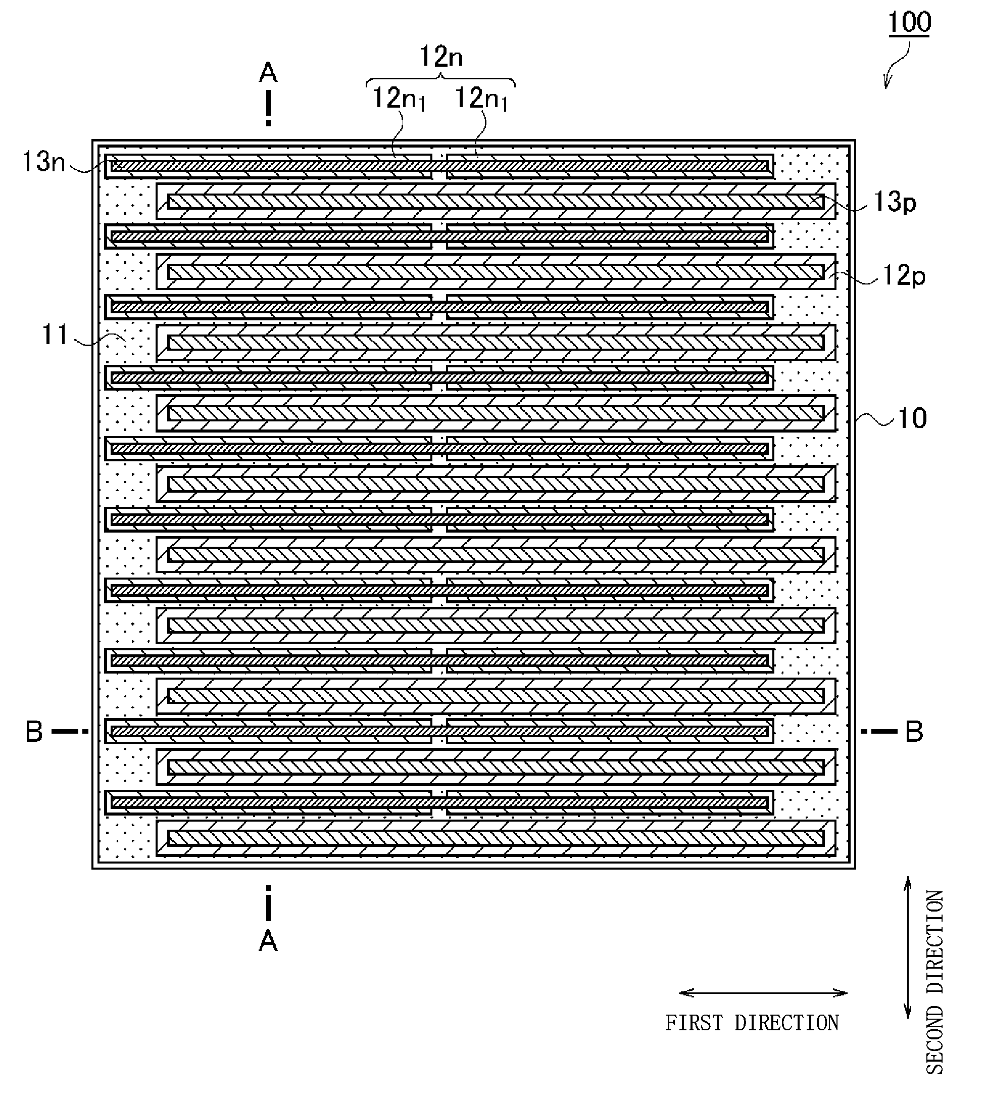
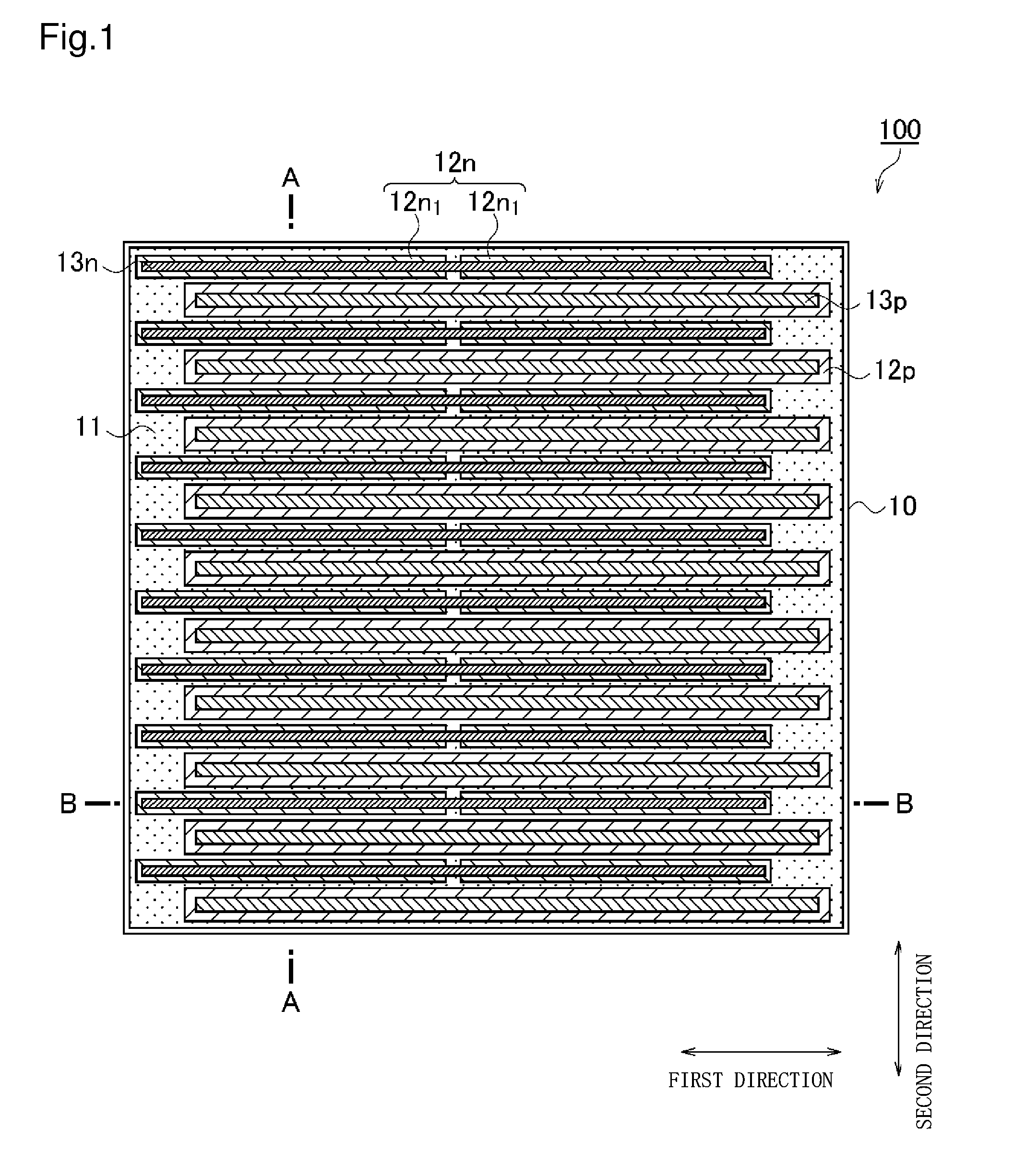
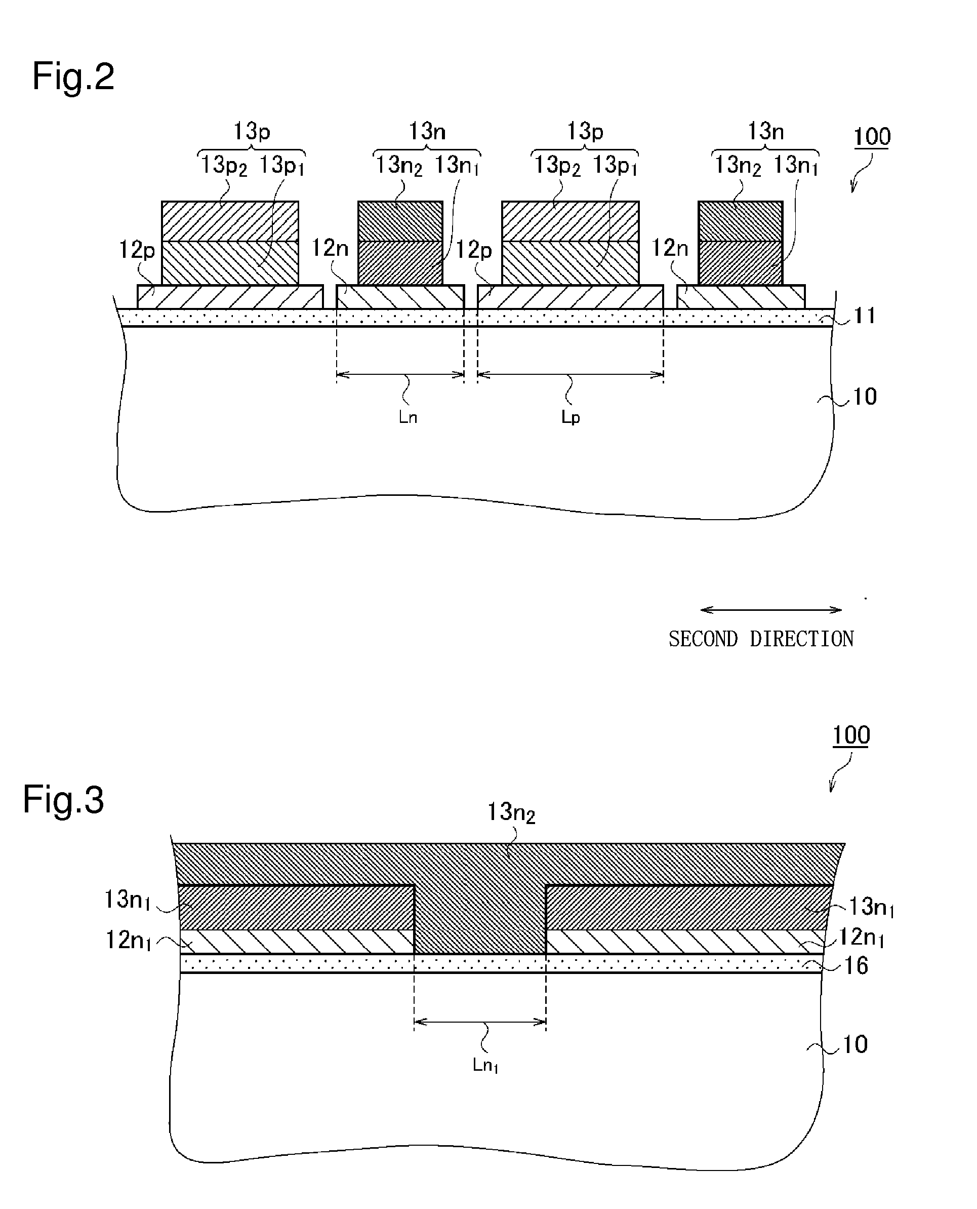
[0025]Descriptions are provided hereinbelow for an embodiment according to the invention based on the drawings. In the respective drawings referenced herein, the same constituents are designated by the same reference numerals and duplicate explanation concerning the same constituents is basically omitted. All of the drawings are provided to illustrate the respective examples only. No dimensional proportions in the drawings shall impose a restriction on the embodiments. For this reason, specific dimensions and the like should be interpreted with the following descriptions taken into consideration. In addition, the drawings include parts whose dimensional relationship and ratios are different from one drawing to another.

[0026]Prepositions, such as “on”, “over” and “above” may be defined with respect to a surface, for example a layer surface, regardless of that surface's orientation in space. The preposition “above” may be used in the specification and claims even if a layer is in cont...


PUM


Abstract

A method of manufacturing a solar cell, including: forming a first conductivity type semiconductor layer extending along a predetermined direction on aback surface of a semiconductor substrate that has a light-receiving surface and the back surface opposite to the light-receiving surface, the first-conductivity-type semiconductor layer being divided into plural island-shaped sections arranged side by side in the predetermined direction; forming a semiconductor layer of a second conductivity type in the predetermined direction on the back surface; and forming conductive layers respectively on the first-conductivity-type semiconductor layer and the second-conductivity-type semiconductor layer by using a conductive paste, the conductive layer to be formed on the first-conductivity-type semiconductor layer being formed by a printing method such that the conductive layer to be formed on the first-conductivity-type semiconductor layer extends on a line of the plural island-shaped sections to bridge adjacent two of the plural island-shaped sections.

Description

CROSS REFERENCE TO RELATED APPLICATIONS[0001]This application claims priority based on 35 USC 119 from prior Japanese Patent Application No. P2008-250737 filed on Sep. 29, 2008, entitled “SOLAR CELL AND METHOD OF MANUFACTURING THE SAME”, the entire contents of which are incorporated herein by referenceBACKGROUND OF THE INVENTION[0002]1. Field of the Invention[0003]The invention relates to aback junction solar cell and a method of manufacturing the solar cell.[0004]2. Description of Related Art[0005]Solar cells are now expected to be a new energy source because of their capability to convert sunlight, which is clean and in unlimited supply, directly into electricity. The output of a single solar cell is only several watts. Accordingly, if solar cells are used as an electric-power source (energy source) for a house, building or the like, a solar cell module is used in which multiple solar cells are electrically connected together to increase the output.[0006]There has been known a so-...

Claims


Application Information

Patent Timeline
Patent Type & Authority Applications(United States)
IPC IPC(8): H01L31/0216H01L31/18
CPCH01L31/022425Y02E10/50H01L31/03529H01L31/022441
Inventor IDE, DAISUKE
Owner PANASONIC INTELLECTUAL PROPERTY MANAGEMENT CO LTD
Why Eureka
Try Eureka