Catadioptric optical system for lithography

Inactive Publication Date: 2000-08-08
ELECTRONICS & TELECOMM RES INST
View PDF8 Cites 5 Cited by
  • Summary
  • Abstract
  • Description
  • Claims
  • Application Information

AI Technical Summary

Benefits of technology

First, as shown in FIG. 1, the radiation from a light source is incident on an enlarged original mask 10 uniformly via an illumination optical system. Information on the mask 10 is then corrected for astigmation by the radiation passing through a first lens group 20. A folding mirror 30 disposed at the rear end of the first lens group 20 changes the direction of radiation by 90 degrees. The radiation passing through a second lens group 40 provides an astigmation control and is focused. A polarized beam splitter 50 disposed at the rear end of the second lens group 40 causes an incident polarized beam from the light source to reflect. A first wave plate 60 is disposed on the polarized beam splitter 50. The first wave plate 60 converts the linearly polarized beam reflected from the polarized beam splitter 50 to a circularly polarized beam. A spherical mirror 70 reflects the circularly polarized beam having passed through the first wave plate 60 to the first wave plate 60. Passing through the first wave plate 60, the circularly polarized beam is changed back to the linearly polarized beam and is incident upon a second wave plate 80 via the polarized beam splitter 50. The second wave plate 80 converts the incident polarized beam to a circularly polarized beam. Passing through the second wave plate 80, the circularly polarized beam provides the final astigmation control, so that the pattern on the mask is transferred to the surface of a wafer 100. This makes it possible to realize fine line width on the wafer. The optical system used herein is a scanning type catadioptric optical system having the exposure area of 26.times.5 mm.sup.2 and using an ArF excimer laser of 193.3 nm in wavelength as a light source, where the magnification of the whole system is 1 / 4 (reduction) and the numerical aperture is 0.55.

Problems solved by technology

An increase in the numerical aperture of optical system is disadvantageous in regards to process and design of the optical system in that the depth of focus becomes small.
However, where a short-wavelength ultraviolet light source is used, there is a limitation upon optical materials.
A conventional dioptric optical system for lithography is constituted by lenses only, and has to employ fused quartz exclusively as an optical material, which causes an astigmation.
Other disadvantages involving such a conventional dioptric optical system are a rapid decline in the total transmittance of the optical system resulting from a loss of light since fused quartz exhibits a high absorptance, and a deterioration of the optical material by light source, thereby causing a defect in the fused quartz and reducing the life of optical system.

Method used


Image

  • Catadioptric optical system for lithography
  • Catadioptric optical system for lithography
  • Catadioptric optical system for lithography

Examples


Embodiment Construction

Hereinafter, the preferred embodiments of the present invention will be described with reference to the accompanying drawings.

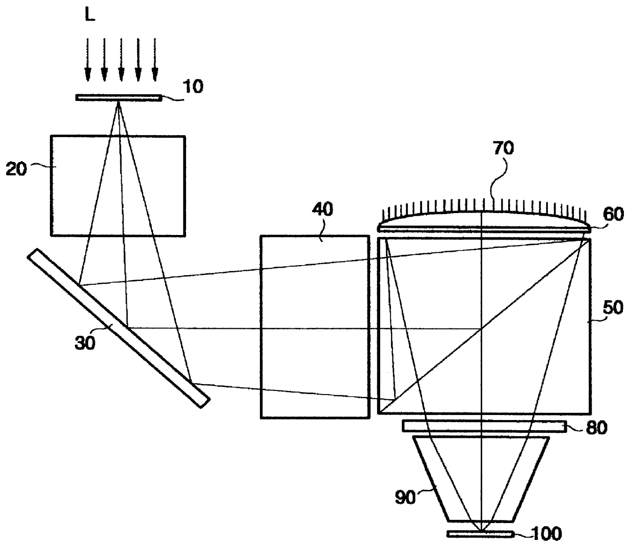
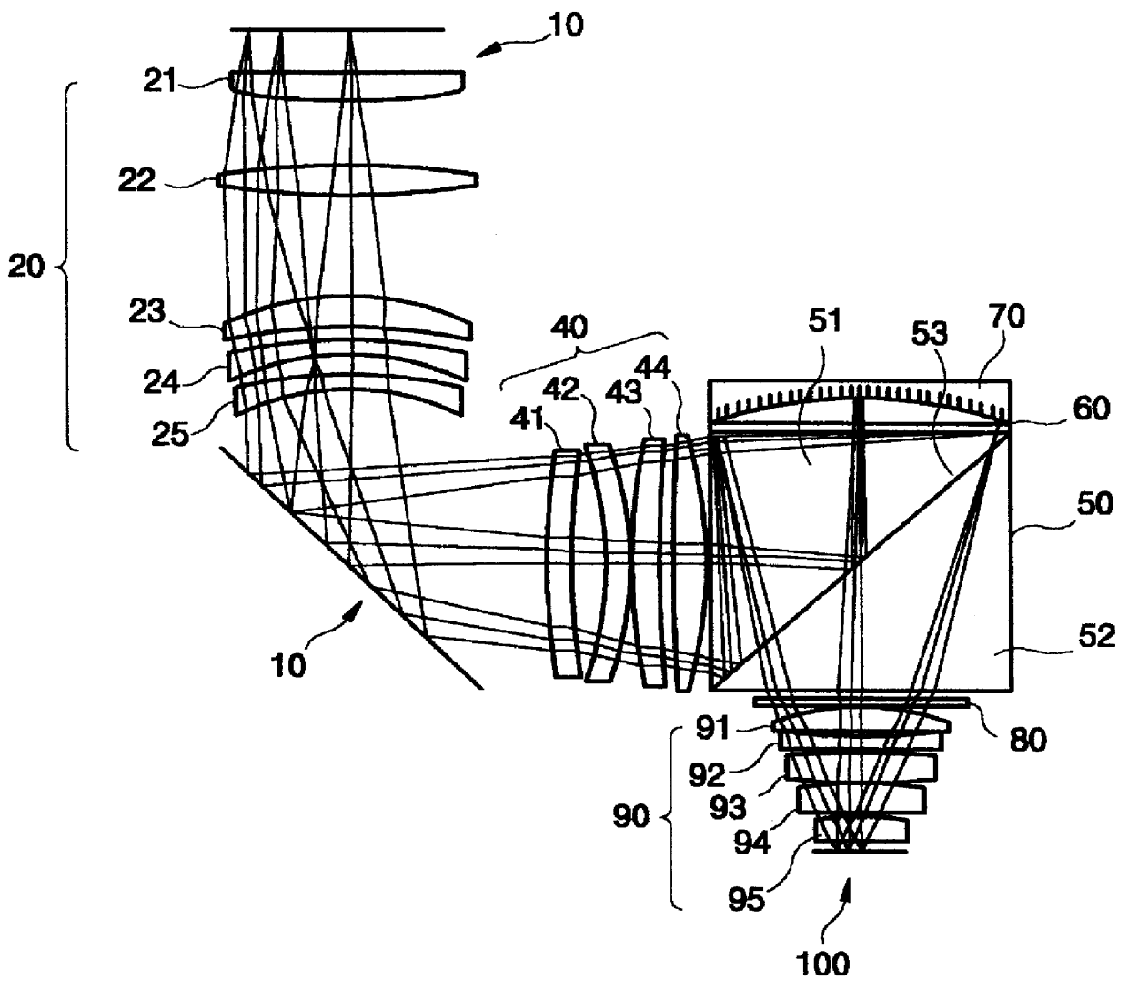
FIG. 1 is a schematic view showing a configuration of a catadioptric optical system in accordance with the present invention.

First, as shown in FIG. 1, the radiation from a light source is incident on an enlarged original mask 10 uniformly via an illumination optical system. Information on the mask 10 is then corrected for astigmation by the radiation passing through a first lens group 20. A folding mirror 30 disposed at the rear end of the first lens group 20 changes the direction of radiation by 90 degrees. The radiation passing through a second lens group 40 provides an astigmation control and is focused. A polarized beam splitter 50 disposed at the rear end of the second lens group 40 causes an incident polarized beam from the light source to reflect. A first wave plate 60 is disposed on the polarized beam splitter 50. The first wave plate 60 converts the...


PUM


Abstract

Provided with an optical system which is applicable to an exposure apparatus used in the manufacture of semiconductors and includes a combination of a spherical mirror having a function of refraction and lenses for astigmation control, using a CaF2 lens as the last lens, thereby making it possible to use a light source operating at a short wavelength and a wide bandwidth, enhance the life of the optical system, and transfer the enlarge pattern of a mask onto the wafer for realizing fine line width.

Description

1. Field of the InventionThe present invention relates to an optical system of exposure apparatuses used in the manufacture of a semiconductor device and, more particularly, to a catadioptric optical system for lithography including a spherical mirror and lenses for transferring a pattern from an enlarged original mask onto a wafer using an ArF excimer laser as a light source, thereby realizing a very fine line width.2. Description of the Prior ArtAs the integration of the semiconductor devices with enlarged capacity has been improved, there is an increase in the demand for a highly fine pattern constituting a circuitry and a large chip size. In order to satisfy such a demand, there have been occurred necessities for higher performance of exposure apparatuses used in the semiconductor exposure process. The line width realized by exposure apparatuses fundamentally depends upon the resolution of optical system. The resolution of optical system in an exposure apparatus is proportional ...

Claims


Application Information

Patent Timeline
IPC IPC(8): G02B17/08G03F7/20
CPCG02B17/08G02B17/0892G03F7/70225
Inventor CHUNG, HAI BINKIM, JONG SOOLEE, KAG HYEONKIM, DOH HOONCHOI, SANG SOOYOO, HYUNG JOUN
Owner ELECTRONICS & TELECOMM RES INST
Why Eureka
Try Eureka