Conductor pattern and electronic component having the same

a technology of electronic components and patterns, applied in the direction of impedence networks, inductances, multiple-port networks, etc., can solve the problems of large chip components, poor electrical characteristics, and smooth processing of data, so as to improve connectivity, improve characteristics and reliability of electronic components, and high resolution

Inactive Publication Date: 2013-02-28
SAMSUNG ELECTRO MECHANICS CO LTD
View PDF4 Cites 6 Cited by
  • Summary
  • Abstract
  • Description
  • Claims
  • Application Information

AI Technical Summary

Benefits of technology

[0020]An object of the present invention is to provide a conductor pattern capable of implementing a conductor pattern having a high-precision fine line width and a high resolution to improve connectivity, thereby improving characteristics and reliability of an electronic component, and an electronic component having the same.

Problems solved by technology

In order to transmit and receive a large amount of data as described above, there is a problem in smoothly processing the data due to signal delay and other noises at the time of transmission and reception of the data of the high frequency band such as the GHz band between a main device and a peripheral device.
However, the existing counter EMI component, which is a winding or multilayered type, has a large chip component and bad electrical characteristics, such that it may be used only in a limited region such as a specific portion, a large area circuit board, and the like.
The existing winding or multilayered type counter EMI components have a limitation in forming an internal circuit having a small area required for adding various functions in order to correspond to formation and miniaturization of an internal conductor pattern and causes many problems.
Here, in the case of directly forming the internal conductor pattern on a magnetic material substrate and a polymer resin insulating layer or the magnetic material substrate, various problems have been generated at the time of performing deposition, exposure, development, plating, and etching processes.
In particular, in the case of removing unnecessary metal patterns in order to implement a fine line width of the internal conductor pattern at the time of performing the etching process, an interval between the patterns adjacent to each other is narrow, such that it is difficult to perform penetration of an etching liquid and delamination, thereby causing problems such as collapse of the patterns, local removal of an actual pattern due to over-etching, and the like.
In addition, product reliability is decreased due to a decrease in adhesion between the internal conductor pattern and the substrate caused by under-cut.
In addition, as shown in FIG. 1C, the thickness of the internal conductor pattern 3 is non-uniform to decrease the adhesion between the substrate and the internal conductor pattern and cause distortion of the pattern due to a step generated at the time of forming a plurality of layers.
Therefore, a treating liquid is not smoothly penetrated or removed at the time of performing the exposure, the development, and the etching processes to decrease implementation of the internal conductor patterns.

Method used


Image

  • Conductor pattern and electronic component having the same
  • Conductor pattern and electronic component having the same
  • Conductor pattern and electronic component having the same

Examples


Embodiment Construction

[0032]Hereinafter, exemplary embodiments of the present invention in which objects of the present invention may be specifically implemented will be described with reference to the accompanying drawings. In the exemplary embodiments of the present invention, the same terms and reference numerals will be used to describe the same components. Therefore, an additional description for the same component will be omitted below.

[0033]Hereinafter, an exemplary embodiment of a common mode filter according to the present invention will be described in detail with reference to FIGS. 4 to 6.

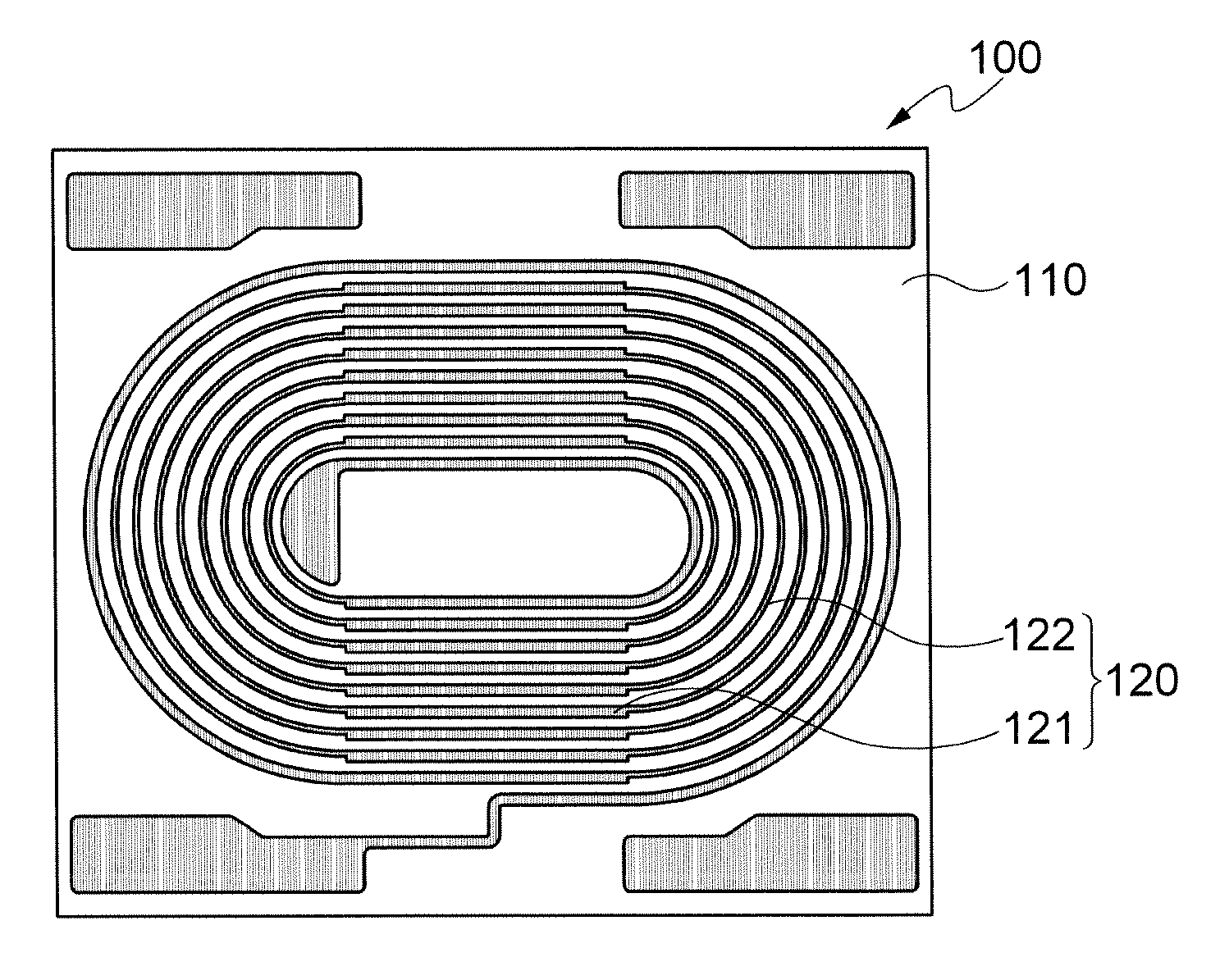
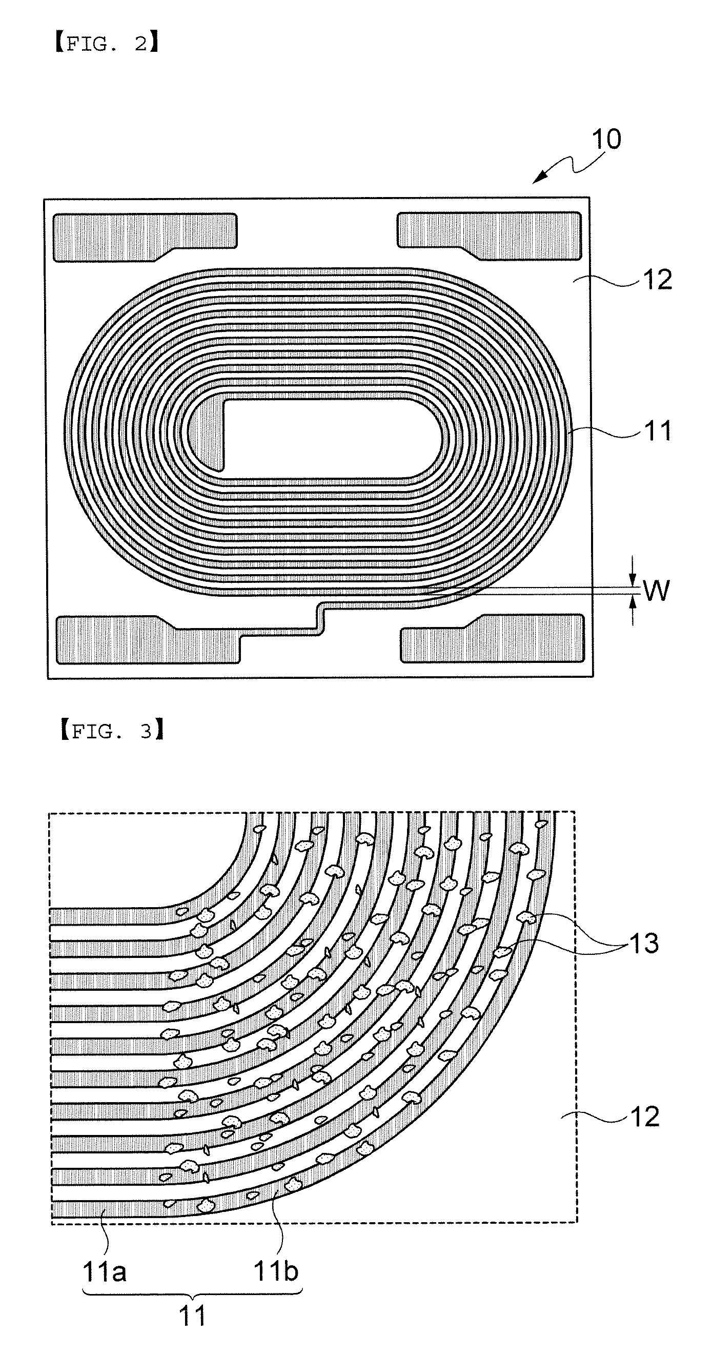
[0034]FIG. 4 is a transverse cross-sectional view schematically showing a common mode filter according to the present invention, FIG. 5 is an enlarged view of a major part schematically showing the internal conductor pattern of the common mode filter according to the present invention, and FIG. 6 is a block diagram schematically showing a process of manufacturing the common mode filter according to the presen...


PUM

PropertyMeasurementUnit
widthaaaaaaaaaa
widthaaaaaaaaaa
width W2aaaaaaaaaa

Abstract

Disclosed herein are a conductor pattern of an electronic component formed in an oval coil shape on a magnetic substrate, the conductor pattern including: a straight part; and a curved part connected to the straight part at both sides thereof, wherein a line width of the curved part is smaller than that of the straight part, and an electronic component including the same. With the conductor pattern and the electronic component including the same according to the present invention, the high precision fine line width and the high resolution conductor pattern may be implemented to improve connectivity, thereby improving characteristics and reliability of the electronic component.

Description

CROSS REFERENCE(S) TO RELATED APPLICATIONS[0001]This application claims the benefit under 35 U.S.C. Section 119 of Korean Patent Application Serial No. 10-2011-0086532, entitled “Conductor Pattern and Electronic Component Having the Same” filed on Aug. 29, 2011, which is hereby incorporated by reference in its entirety into this application.BACKGROUND OF THE INVENTION[0002]1. Technical Field[0003]The present invention relates to a conductor pattern and an electronic component having the same, and more particularly to a conductor pattern capable of implementing a conductor pattern having a high precision fine line width and a high resolution to improve connectivity, thereby improving characteristics and reliability of an electronic component, and an electronic component having the same.[0004]2. Description of the Related Art[0005]In an electronic component such as a digital TV, a smart phone, a laptop computer, or the like, a transmission / reception function of data in a high frequenc...

Claims


Application Information

Patent Timeline
Patent Type & Authority Applications(United States)
IPC IPC(8): H01F5/00
CPCH01F17/0006H01F2017/0073H01F2017/0066H01F41/041H01F17/00H01F27/00H03H7/09
Inventor KIM, YONG SUKWI, SUNG KWONLEE, SANG MOONYOO, YOUNG SEUCKKWAK, JEONG BOK
Owner SAMSUNG ELECTRO MECHANICS CO LTD
Why Eureka
Try Eureka