Flip-chip package structure, and the substrate and the chip thereof

a technology of packaging substrate and chip, applied in the direction of printed circuit aspects, sustainable manufacturing/processing, final product manufacturing, etc., can solve the problems of increasing complexity, increasing the function and strength of the semiconductor chip formed by forming atop the semiconductor chip, and reducing the height of the interval between the packaging substrate and the chip

Inactive Publication Date: 2009-01-15
PHOENIX PRECISION TECH CORP
View PDF2 Cites 6 Cited by
  • Summary
  • Abstract
  • Description
  • Claims
  • Application Information

AI Technical Summary

Benefits of technology

[0010]An object of the present invention is to provide a flip-chip package structure, which can provide a semiconductor chip package with characteristics of fine line width and fine line pitch.
[0011]Another object of the present invention is to provide a flip-chip package structure, which is able to improve the thermo stress of the flip-chip package structure, improve the quality of underfill material filling, and enhance the reliability of the flip-chip package structure.

Problems solved by technology

As performance of semiconductor processes advances, semiconductor chips formed thereby have more and stronger functions and tend towards complexity.
As chip techniques have developed towards high work frequency and larger amounts of I / O contact pads, conventional wire bonding has failed to satisfy demands of conductivity.
Although such structure and the method of providing the same can be used for electrical conduction, it has restrictions when the character of fine line width and fine line pitch is required.
However, when the size of the solder bumps 25 is smaller, the height of the interval between the packaging substrate and the chip is decreased, which further results in unusual filling of the underfill material and the occurrence of voids in the underfill material when it fills in the interval between the packaging substrate and the chip.
Also, serious problems such as cracking of the packaging substrate will possibly occur and result in deterioration of the reliability.
Consequently, the conventional method of forming the bump is not suitable for the producing of the IC packaging substrate having fine line width and fine line pitch.

Method used


Image

  • Flip-chip package structure, and the substrate and the chip thereof
  • Flip-chip package structure, and the substrate and the chip thereof
  • Flip-chip package structure, and the substrate and the chip thereof

Examples


example 1

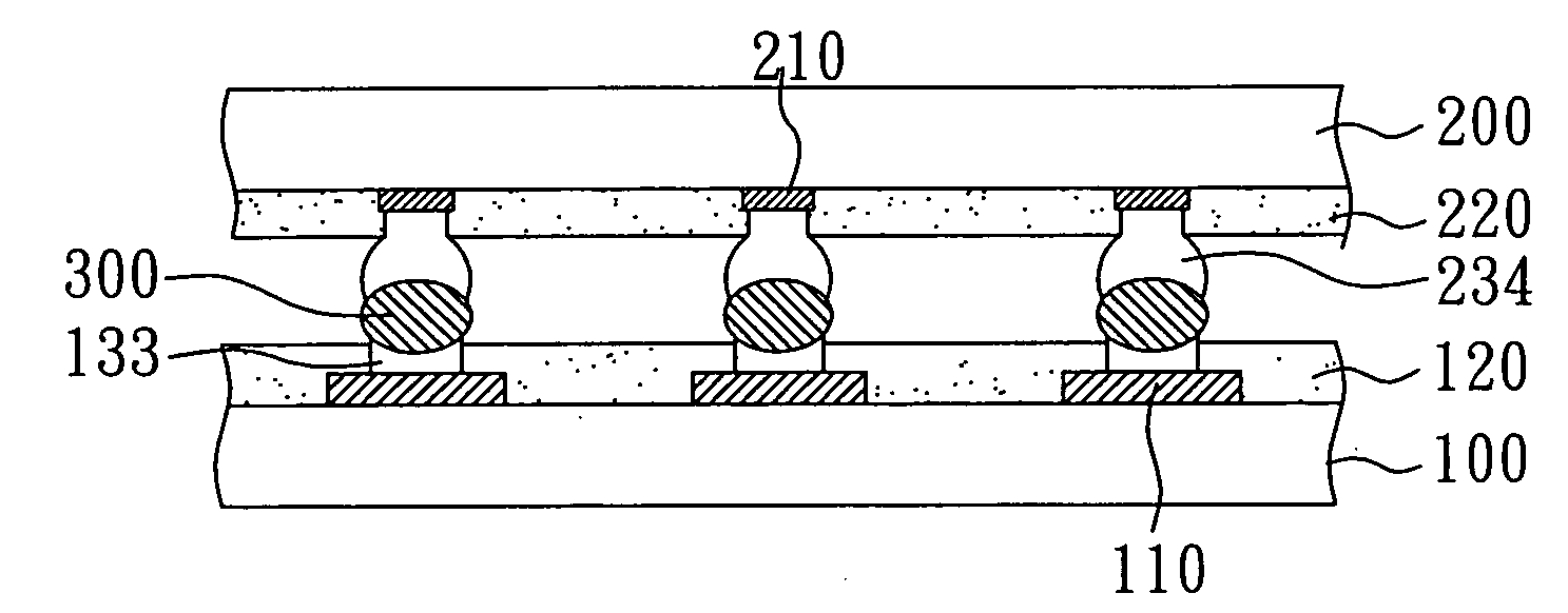
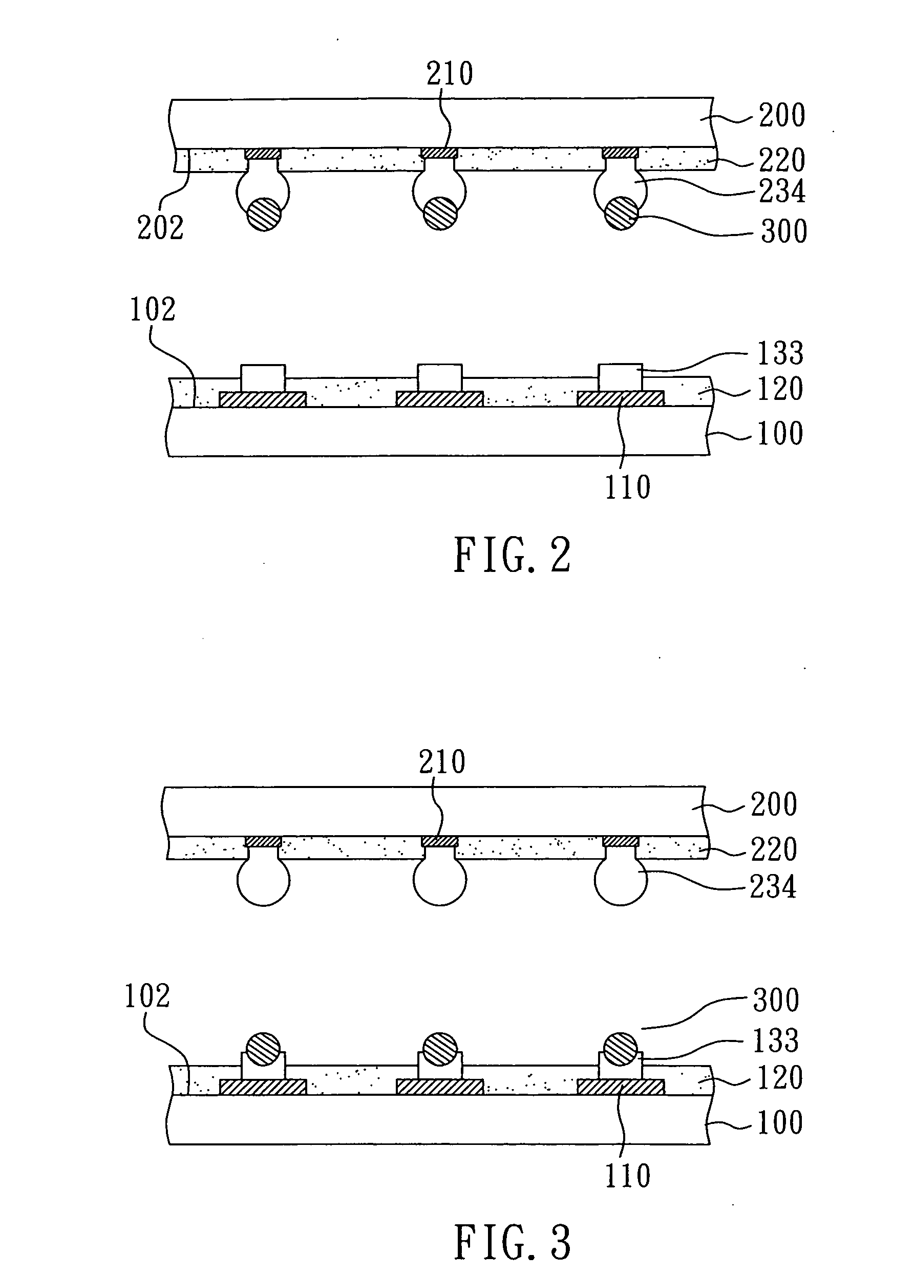
[0041]Referring to FIG. 2, the flip-chip package structure of the present Example 1 comprises: a packaging substrate 100 and a semiconductor chip 200. A plurality of conductive pads 110 and a solder mask 120 are formed on the upper surface 102 of the substrate 100, a plurality of openings is formed in the solder mask 120 to expose the conductive pads 110, and a plurality of third solder bumps 133 is provided on the conductive pads 110 correspondingly. A plurality of electrode pads 210 and a passivation layer 220 covering the active surface 202 of the semiconductor chip 200, in which the passivation layer 220 has a plurality of openings to expose the electrode pads 210. Second solder bumps 234 are located on the electrode pads 210 correspondingly. Further, solid grains 300 are located on the second solder bumps 234, wherein the diameter of the solid grain 300 is smaller than the width of the second solder bump 234.

[0042]In the present example, the solid grain 300 can be a hard metal ...

example 2

[0049]Referring to FIG. 6, the flip-chip package structure according to the present example includes a packaging substrate 100 and a semiconductor chip 200. A plurality of conductive pads and 110 and a solder mask 120 are formed on the upper surface 102 of the packaging substrate 100, a plurality of openings is formed in the solder mask 120 to expose the conductive pads 110, and a plurality of third solder bumps 133 is provided on the conductive pads 110 correspondingly. A plurality of electrode pads 210 and a passivation layer 220 covering the active surface 202 of the semiconductor chip 200, in which the passivation layer 220 has a plurality of openings to expose the electrode pads 210. Second solder bumps 234 are located on the electrode pads 210 correspondingly. Further, solid grains 300 are located on the second solder bumps 234, wherein the diameter of the solid grain 300 is larger than the width of the second solder bump 234.

[0050]In the present example, the solid grain 300 i...


PUM


Abstract

A flip-chip package structure is disclosed, which comprises: a packaging substrate having an upper surface and a plurality of conductive pads formed on the upper surface; a semiconductor chip having an active surface and a plurality of electrode pads formed on the active surface; and a plurality of first solder bumps; wherein each first solder bump connects to an electrode pad and a conductive pad, and each first solder bump contains a solid grain.

Description

BACKGROUND OF THE INVENTION[0001]1. Field of the Invention[0002]The present invention relates to a flip-chip package structure and, more particularly, to a flip-chip package structure with fine line width and fine line pitch.[0003]2. Description of Related Art[0004]As performance of semiconductor processes advances, semiconductor chips formed thereby have more and stronger functions and tend towards complexity. At the same time, amounts of transmission data of semiconductors increase more and more. Therefore, quantities of I / O (inputs / outputs) contact pads of semiconductor chips have to increase in accordance with the above-mentioned.[0005]As chip techniques have developed towards high work frequency and larger amounts of I / O contact pads, conventional wire bonding has failed to satisfy demands of conductivity. Compared with conventional wire bonding, a flip-chip package process is a technique that a chip faces downward to conduct a packaging substrate by means of solder bumps. Besi...

Claims


Application Information

Patent Timeline
Patent Type & Authority Applications(United States)
IPC IPC(8): H01L23/52
CPCH01L24/10H01L2224/0558H01L2224/1308H01L2224/13082H01L2224/131H01L2224/13111H01L2224/13116H01L2224/13139H01L2224/13147H01L2224/16H01L2224/81193H01L2224/8121H01L2224/81815H01L2924/01013H01L2924/01029H01L2924/01082H05K3/3436H05K2201/10234H05K2201/10977H05K2201/10992H05K2203/041H01L24/81H01L2224/05624H01L24/13H01L2224/0401H01L2924/0105H01L2924/01047H01L2924/01033H01L2924/01006H01L2924/00013H01L2924/00014H01L2924/014H01L2224/13099H01L2924/00H01L24/05H01L2224/05647H01L2224/13Y02P70/50
Inventor HSU, SHIH-PING
Owner PHOENIX PRECISION TECH CORP
Why Eureka
Try Eureka