Method For Forming Package Substrate With Ultra-Thin Seed Layer

a technology of package substrate and seed layer, which is applied in the direction of printed circuit, electrical apparatus, printed circuit aspects, etc., can solve the problems of low low wiring density, and achieve the effect of increasing the yield of package substrate with fine circuit lines

Inactive Publication Date: 2013-03-21
KINSUS INTERCONNECT TECH
View PDF2 Cites 6 Cited by
  • Summary
  • Abstract
  • Description
  • Claims
  • Application Information

AI Technical Summary

Benefits of technology

[0006]An objective of the present invention is to provide a method for forming a package substrate with an ultra-thin seed layer, which comprises: laminating a metal foil onto a substrate; forming at least one via hole through the substrate and the metal foil; etching away the metal foil, so that the substrate has a rough surface; forming a seed layer on the rough surface of the substrate and an sidewall of the at least one via hole, the seed layer being made of electrically conductive material; laminating a dry film onto the seed layer wherein the dry film has a plurality of openings exposing a portion of the seed layer and the at least one via hole; plating a metal to fill the at least one via hole and on the portion of the seed layer exposed by the openings of the dry film so as to form at least one metal bump on the portion of the seed layer, and on the at least one via hole filled with the metal; and removing the dry film and the seed layer outside the at least one metal bump, wherein the seed layer is formed along the rough surface of the substrate, so that the seed layer also has a rough surface, and the adhesion of the at least one metal bump and / or the circuits, and the substrate is increased through the rough surface of the seed layer. Furthermore, because the seed layer is ultra thin, the metal bumps or the circuit lines formed on the package substrate can be made finer in line widths and line pitches, and the good yield of the package substrate with fine circuit lines can be increased.
[0007]Another objective of the present invention is to provide a method for forming a package substrate with an ultra-thin seed layer, which comprises: laminating a first metal foil and a second metal foil onto a top surface and a bottom surface of the substrate, respectively; forming at least one via hole through the substrate, the first metal foil, and the second metal foil; etching away the first metal foil and the second metal foil, so that the substrate has a rough top surface and a rough bottom surface; forming a seed layer on the rough top surface, the rough bottom surface, and an sidewall of the at least one via hole, the seed layer being made of electrically conductive material; laminating a first dry film onto the seed layer on the rough top surface, and laminating a second dry film onto the seed layer on the rough bottom surface, wherein the first and second dry films each has a plurality of openings exposing a portion of the seed layer and the at least one via hole; plating a metal to fill the at least one via hole and on the portion of the seed layer exposed by the openings of the first and second dry films so as to form at least one metal bump on the portion of the seed layer, and on the at least one via hole filled with the metal; and removing the first and second dry films and the seed layer outside the at least one metal bump to form the package substrate having a double-layer structure, wherein the seed layer is formed along the rough surface of the substrate, so that the seed layer also has a rough surface, and the adhesion of the at least one metal bump and / or the circuits, and the substrate is increased through the rough surface of the seed layer. Furthermore, because the seed layer is ultra thin, the metal bumps or the circuit lines formed on the package substrate can be made finer in line widths and line pitches, and the good yield of the package substrate with fine circuit lines can be increased.
[0009]In the present invention, the ultra-thin seed layer is used in the package substrate instead of the metal foil used in the conventional package substrate. Because the seed layer is ultra thin, the metal bumps or the circuit lines formed on the package substrate can be made finer in line widths and line pitches, and the good yield of the package substrate with fine circuit lines can be increased. Moreover, in the present invention, the seed layer made of electrically conductive material has a rough surface, and thereby the adhesion of the metal bumps and / or the circuits, and the substrate is increased through the rough surface of the seed layer. Therefore, the adhesion problem between some metal materials and the substrate can be solved.

Problems solved by technology

However, the thickness of the copper foil, which is conventionally served as a conductive layer, is between 3 to 12 μm so that the shortening of metal line pitches is restricted, and thereby the wiring density and the good yield of the substrate with fine circuit lines cannot be increased.

Method used


Image

  • Method For Forming Package Substrate With Ultra-Thin Seed Layer
  • Method For Forming Package Substrate With Ultra-Thin Seed Layer
  • Method For Forming Package Substrate With Ultra-Thin Seed Layer

Examples


first embodiment

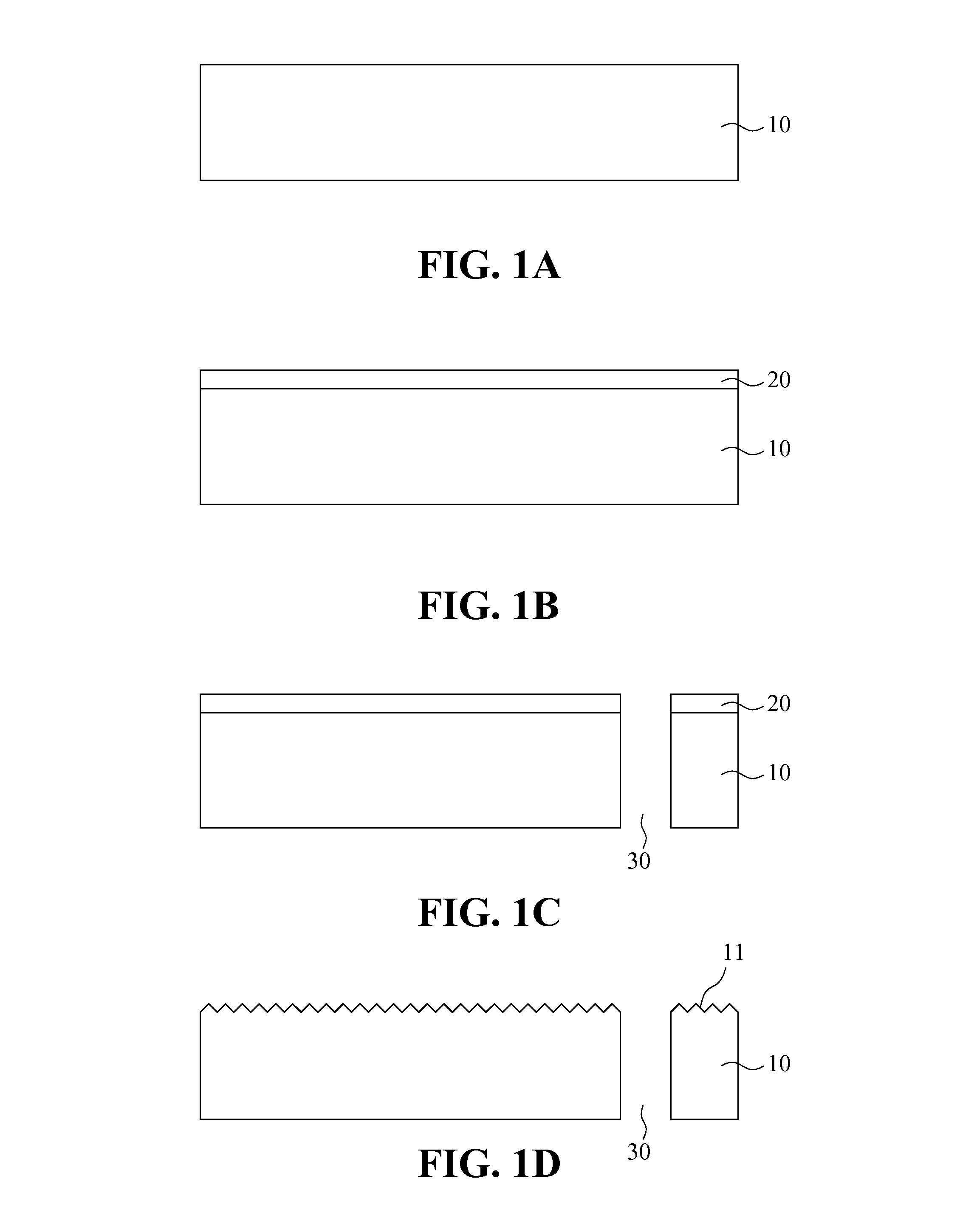
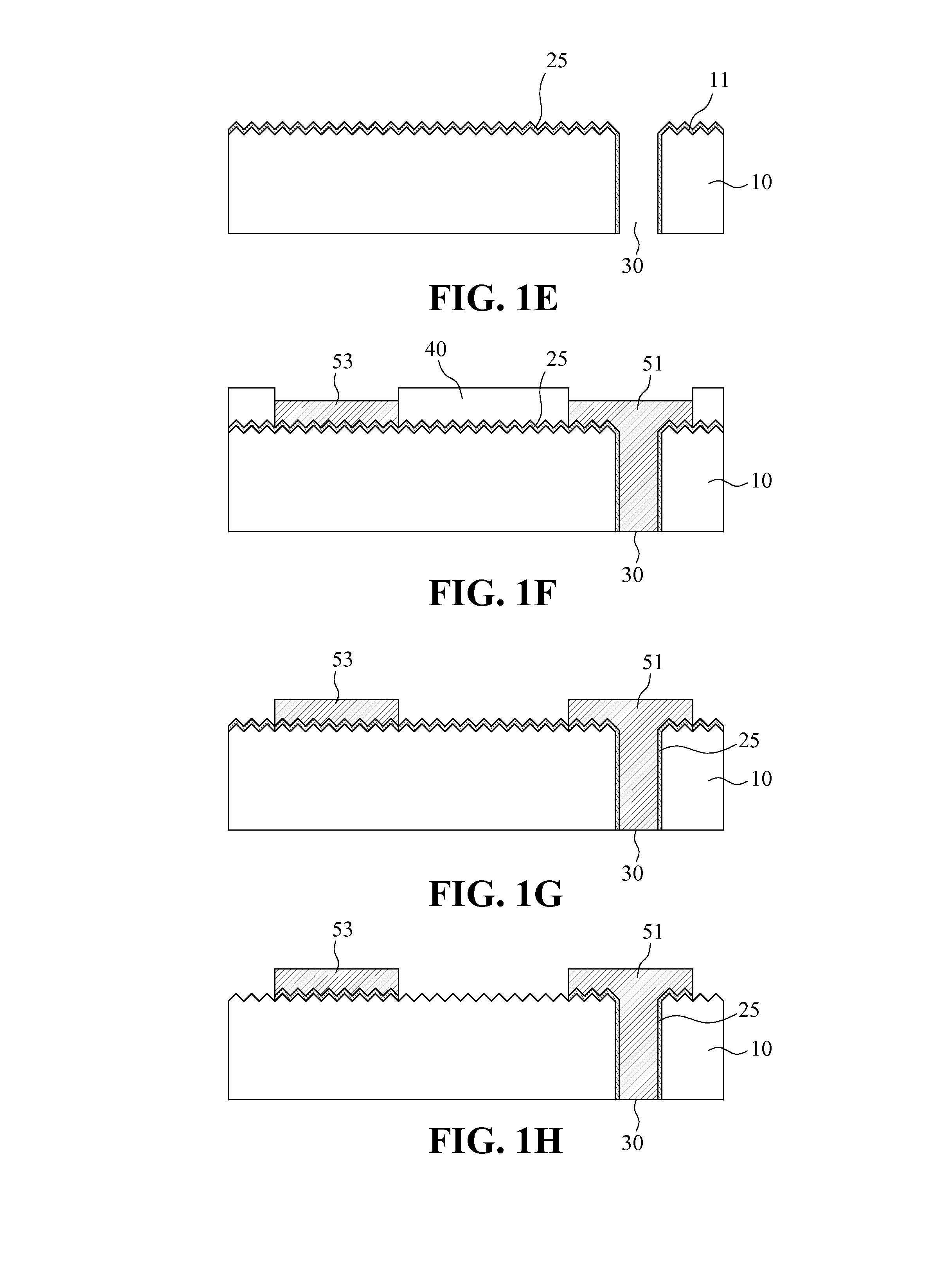
[0015]FIGS. 1A to 1H are cross-sectional views illustrating a method of forming a package substrate with an ultra-thin seed layer according to the present invention. Referring to FIGS. 1A to 1 H, a metal foil 20 is laminated on a surface of a substrate 10. Then, at least one via hole 30 (for example, via hole 30 as shown in FIG. 1C) is formed through the substrate 10 and the metal foil 20. Subsequently, the metal foil 20 is etched away, so that the substrate 10 has a rough surface 11. In other words, when the metal foil 20 is etched away from the substrate 10, the surface of the substrate 10 becomes rough, as shown in FIG. 1D.

[0016]Then, an ultra-thin seed layer 25 is formed on the rough surface 11 of the substrate 10 and an sidewall of the at least one via hole 30, and the ultra-thin seed layer 25 is made of electrically conductive material. The ultra-thin seed layer 25 is formed along the rough surface 11 of the substrate 10, and thereby the ultra-thin seed layer 25 also has a rou...

second embodiment

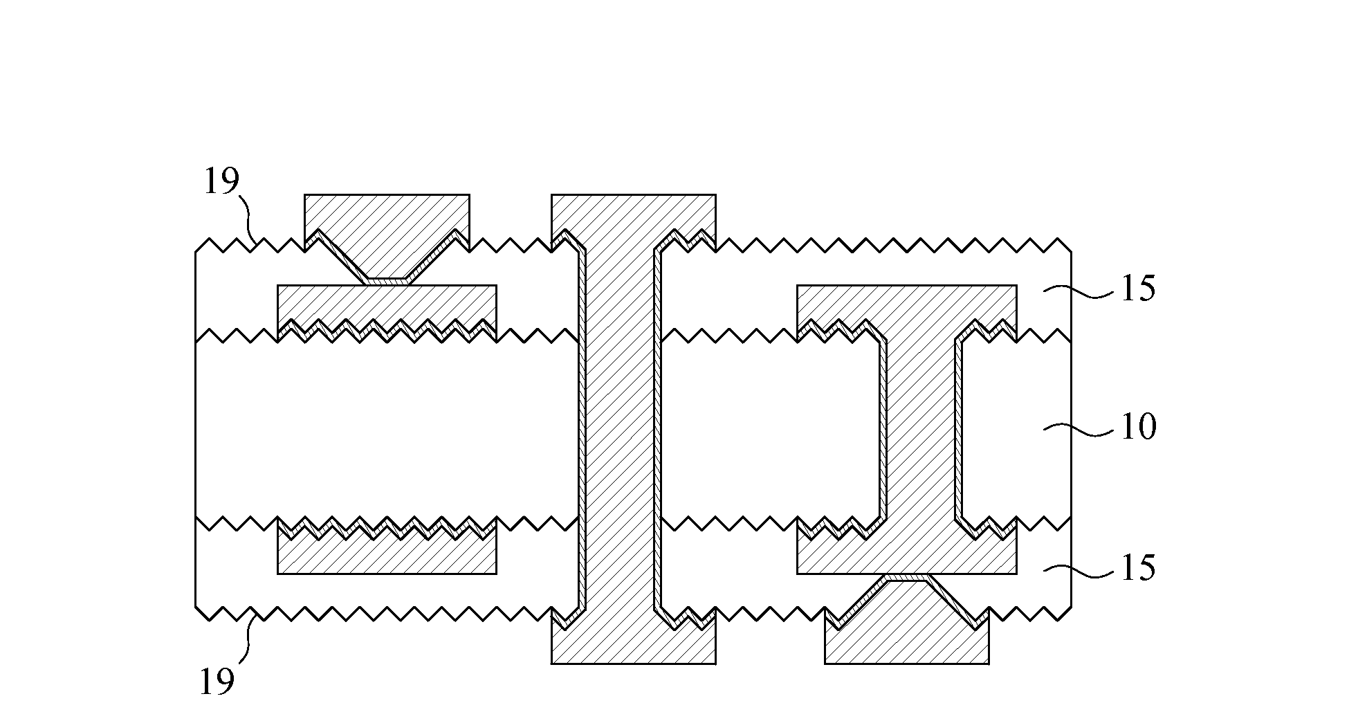
[0019]FIGS. 2A to 2G are cross-sectional views illustrating a method of forming a package substrate with an ultra-thin seed layer according to the present invention. Referring to FIGS. 2A to 2G, a first metal foil 22 and a second metal foil 24 are laminated onto a top surface and a bottom surface of the substrate 10, respectively. Then, at least one via hole 35 (for example, via hole 35 as shown in FIG. 2B) is formed through the substrate 10, the first metal foil 22, and the second metal foil 24. Subsequently, the first metal foil 22 and the second metal foil 24 are etched away, so that the substrate has a rough top surface 13 and a rough bottom surface 15. In other words, when the first metal foil 22 and the second metal foil 24 are etched away from the substrate 10, the top and bottom surfaces 13 and 15 of the substrate 10 become rough, as shown in FIG. 2C.

[0020]Then, an ultra-thin seed layer 27 is formed on the rough top surface 13 and the rough bottom surface 15 of the substrate...


PUM

PropertyMeasurementUnit
thicknessaaaaaaaaaa
thicknessaaaaaaaaaa
electrically conductiveaaaaaaaaaa

Abstract

A method for forming a package substrate with a seed layer is provided, which includes a step of etching away the metal foil laminated on the substrate, so that the substrate has a rough surface, and a step of forming an ultra-thin seed layer on the rough surface of the substrate, wherein the ultra-thin seed layer is formed along the rough surface of the substrate, and thereby the ultra-thin seed layer has a rough surface. Consequently, the adhesion between the metal bumps or circuits formed on the ultra-thin rough seed layer and the substrate can be increased. Furthermore, because the seed layer is ultra thin, the metal bumps or the circuit lines formed on the package substrate can be made finer in line widths and line pitches, and the good yield of the package substrate with fine circuit lines can be increased.

Description

BACKGROUND OF THE INVENTION[0001]1. Field of the Invention[0002]The present invention relates to a method for forming a package substrate, and more particularly to a method for forming a package substrate with an ultra-thin seed layer for increasing the adhesion between the package substrate and the metal bumps or the circuit lines. Accordingly, the metal bumps or the circuit lines on the package substrate can be made finer in line widths and line pitches because the seed layer is ultra thin.[0003]2. The Prior Arts[0004]In a conventional method for forming package substrate, a 3 to 12 μm of thickness of copper foil is directly bonded to the surface of the substrate as a conductive layer, and followed by photolithography, plating and etching to form the circuits. Then, the dry films and the conductive layer uncovered by the circuits are removed. Recently, the printed circuit boards are developed toward lightweight, thin, short and small size, and high density. Therefore, the demand f...

Claims


Application Information

Patent Timeline
Patent Type & Authority Applications(United States)
IPC IPC(8): H01L21/60
CPCH05K3/381H05K3/426H05K2201/09563H05K3/4644H05K3/429
Inventor TSENG, BO-YU
Owner KINSUS INTERCONNECT TECH
Why Eureka
Try Eureka