Solid-state imaging device, imaging apparatus, and ad conversion gain adjusting method

a technology of solid-state imaging and gain adjustment, which is applied in the direction of color signal processing circuits, television system scanning details, television systems, etc., can solve problems such as circuit size increase, and achieve the effect of reducing the problem of circuit size increas

Active Publication Date: 2010-04-01
SONY CORP
View PDF10 Cites 53 Cited by
  • Summary
  • Abstract
  • Description
  • Claims
  • Application Information

AI Technical Summary

Benefits of technology

[0018]According to the embodiment, it is possible to individually perform AD conversion gain adjustment of the reference signal comparison t...

Problems solved by technology

As a result, a circuit size ...

Method used


Image

  • Solid-state imaging device, imaging apparatus, and ad conversion gain adjusting method
  • Solid-state imaging device, imaging apparatus, and ad conversion gain adjusting method
  • Solid-state imaging device, imaging apparatus, and ad conversion gain adjusting method

Examples


first embodiment

Basic Operation: First Embodiment

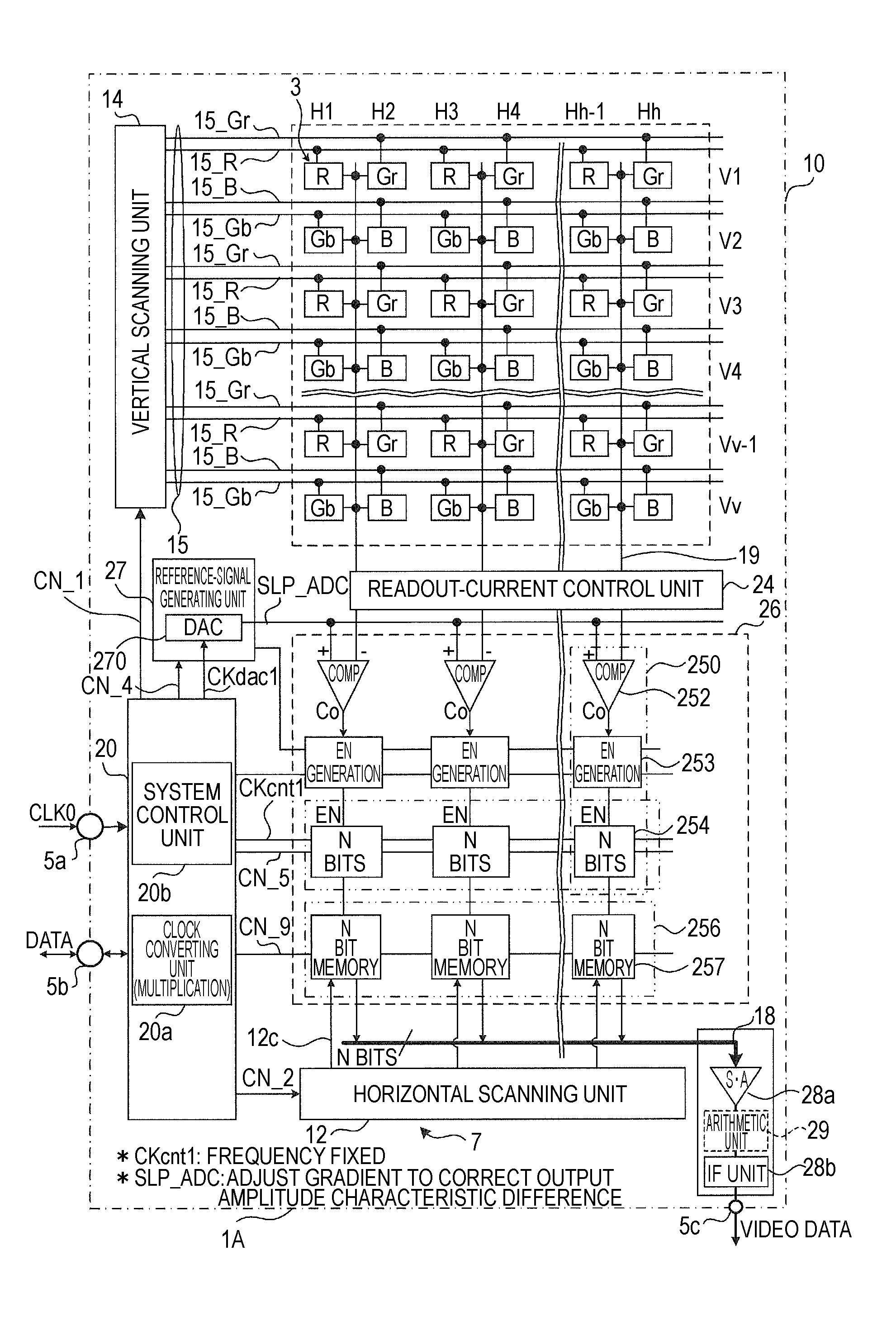
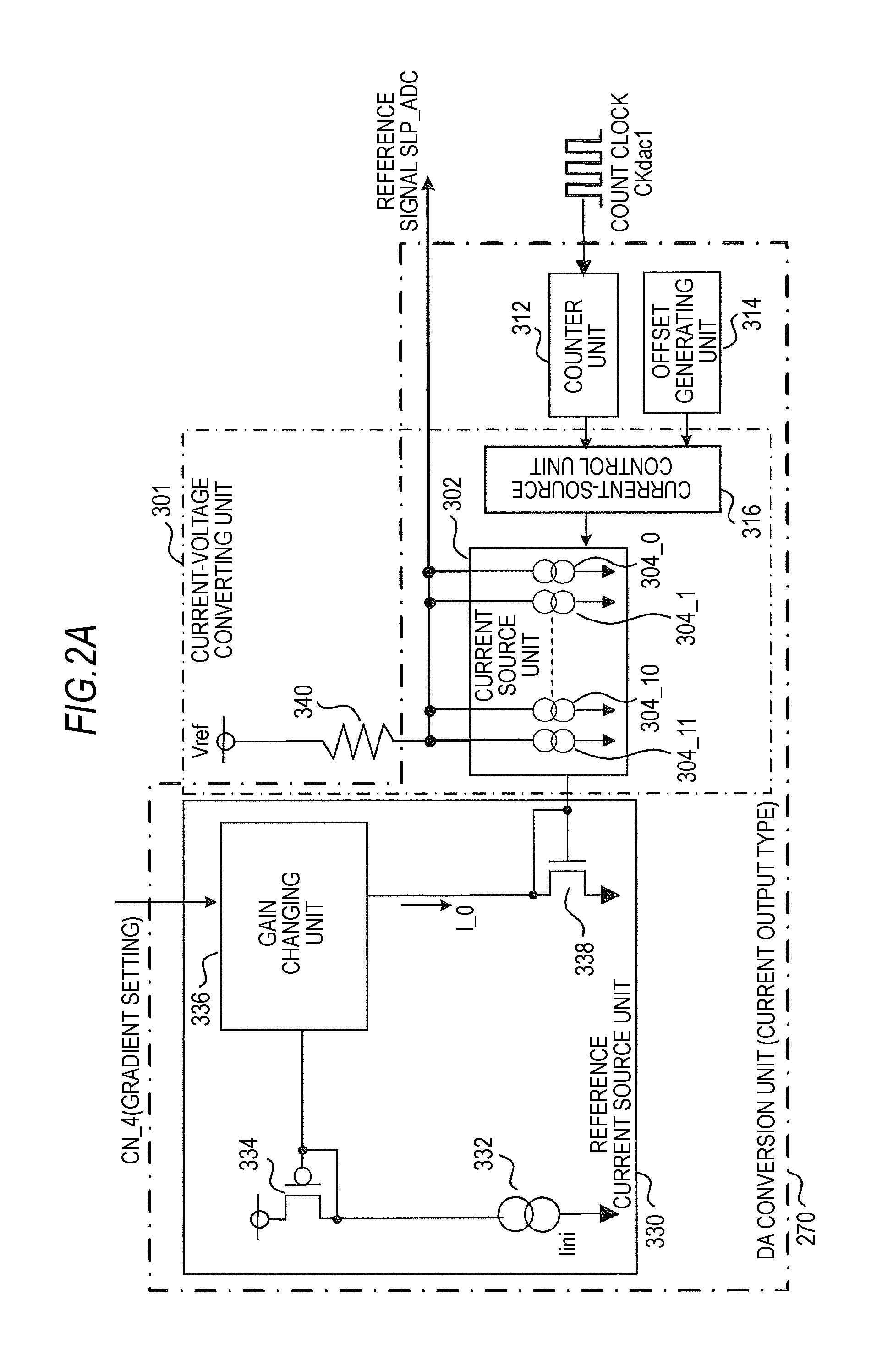
[0118]FIGS. 3A and 3B are diagrams for explaining basic operation of the solid-state imaging device 1A according to the first embodiment. FIG. 3A is a simple circuit diagram of the solid-state imaging device 1A with attention paid to AD conversion processing and CDS processing. FIG. 3B is a timing chart for explaining AD conversion processing in the solid-state imaging device 1A according to the first embodiment.

[0119]As shown in FIG. 3A, as an example, the pixel unit 3 includes, besides a charge generating unit 32, four transistors (a readout selection transistor 34, a reset transistor 36, a vertical selection transistor 40, and an amplification transistor 42) as basic elements included in the pixel-signal generating unit 5. The readout selection transistor 34 included in a transfer unit is driven by a transfer signal TRG via a transfer wire line 54. The reset transistor 36 included in an initializing unit is driven by a reset signal RST via a reset...

first example

[0143]FIG. 4A is a timing chart for explaining AD conversion processing with attention paid to white balance adjusting operation of a first example in the solid-state imaging device 1A according to the first embodiment.

[0144]Pixel signal voltages Vx of the unit pixels 3 in which the color separation filers including three color components of R, G (Gr, Gb), and B are arranged are sequentially read out at different times. For example, concerning the row direction, in odd number rows, first, only the row control lines for R 15_R are controlled, whereby pixel signal voltages Vx_R are simultaneously supplied from all the unit pixels 3 for R in the odd number rows to the column AD processing unit 26. Thereafter, when only the row control lines for Gr 15_Gr are controlled, pixel signal voltages Vx_Gr are simultaneously supplied from all the unit pixels 3 for Gr in the odd number rows to the column AD processing unit 26.

[0145]Subsequently, the solid-state imaging device 1A shifts to readout...

second example

[0165]FIG. 4B is a timing chart for explaining AD conversion processing with attention paid to white balance adjusting operation of a second example in the solid-state imaging device 1A according to the first embodiment.

[0166]In the white balance adjusting operation according to the first embodiment (the first example, Gr and Gb are treated as pixels having the color information of the same color G. When AD conversion for the pixel signal voltages Vx_Gr and Vx_Gb of Gr and Gb is performed, the same value is used for gain setting for white balance adjustment. Gain setting for the four unit pixels 3 forming the color separation filter of the Bayer array only has to be performed for the three colors R, G, and B. There is an advantage that gain setting control is simpler than individually setting gains for the four unit pixels 3.

[0167]However, because of refining of unit pixels, a difference between pixel layout patterns for Gr and Gb, and the like, when light having the same light amou...


PUM


Abstract

A solid-state imaging device includes: a pixel unit in which unit pixels outputting processing target signals are arranged in a horizontal direction and scanning lines are wired such that the processing target signals can be read out in order in a vertical direction within a repetition unit of an array of the unit pixels in the horizontal direction; an AD conversion unit including comparing units that compare a reference signal supplied from a reference-signal generating unit and the processing target signals, and counter units that perform count operation, the AD conversion unit performing AD conversion processing based on output data of the counter units; and a driving control unit that performs control to read out the processing target signals in order in the vertical direction and controls the reference-signal generating unit and the AD conversion unit such that AD conversion gains are individually adjusted in order to correct an output amplitude characteristic difference within the repetition unit during AD conversion processing.

Description

BACKGROUND OF THE INVENTION[0001]1. Field of the Invention[0002]The present invention relates to a solid-state imaging device, an imaging apparatus, and an AD conversion gain adjusting method.[0003]2. Description of the Related Art[0004]For example, in the field of video apparatuses, CCD (Charge Coupled Device), MOS (Metal Oxide Semiconductor), or CMOS (Complementary Metal-Oxide Semiconductor) solid-state imaging devices that detect light (an example of an electromagnetic wave) among physical quantities are used. The solid-state imaging devices read out, as an electric signal, a physical quantity distribution converted into the electric signal by unit components (pixels in the solid-state imaging devices).[0005]There is also an amplification solid-state imaging device including pixels of an amplification solid-state imaging element (APS: Active Pixel Sensor / also referred to as gain cell) configuration having a driving transistor for amplification in a pixel-signal generating unit th...

Claims


Application Information

Patent Timeline
IPC IPC(8): H04N5/228H04N5/335H04N5/365H04N5/374H04N5/378H04N9/04H04N9/07
CPCH04N5/374H04N9/045H04N5/378H04N25/70H04N25/76H04N25/134H04N25/75
Inventor SUZUKI, ATSUSHINITTA, YOSHIKAZU
Owner SONY CORP
Why Eureka
Try Eureka