Photoelectric conversion device and method for making the same

a conversion device and photoelectric technology, applied in the direction of radio frequency controlled devices, television systems, television system scanning details, etc., can solve the problems of difficult oblique light entering the design flexibility of the wiring layout of the mos-type photoelectric conversion device is further degraded, and the light collection efficiency of the photoelectric conversion element is improved, and the increase in the thickness of the insulating film can be suppressed. , the effect of reducing the design flexibility

Inactive Publication Date: 2010-04-01
CANON KK
View PDF3 Cites 13 Cited by
  • Summary
  • Abstract
  • Description
  • Claims
  • Application Information

AI Technical Summary

Benefits of technology

[0009]The present invention provides a photoelectric conversion device in which the light collecting efficiency on a photoelectric conversion element is improved without decreasing the design flexibility of the wiring layout and a method for making a photoelectric conversion device by which an increase in the thickness of the insulating films can be suppressed.

Problems solved by technology

Moreover, since a MOS-type photoelectric conversion device requires a larger number of wiring layers than a CCD-type photoelectric conversion device, the flexibility of designing the wiring layout is low.
Thus, when the pixels are miniaturized, the design flexibility of the wiring layout of the MOS-type photoelectric conversion device is further degraded.
Even when the aperture is made wide, it is difficult for oblique light to enter the photoelectric conversion element if the distance between the photoelectric conversion element and the aperture is large.
This decreases the light collecting efficiency on the photoelectric conversion element.

Method used


Image

  • Photoelectric conversion device and method for making the same
  • Photoelectric conversion device and method for making the same
  • Photoelectric conversion device and method for making the same

Examples


first embodiment

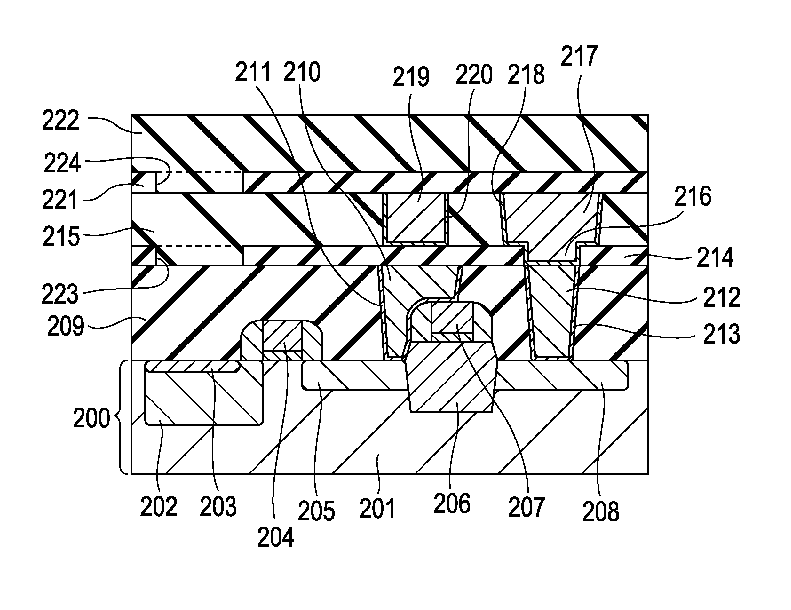
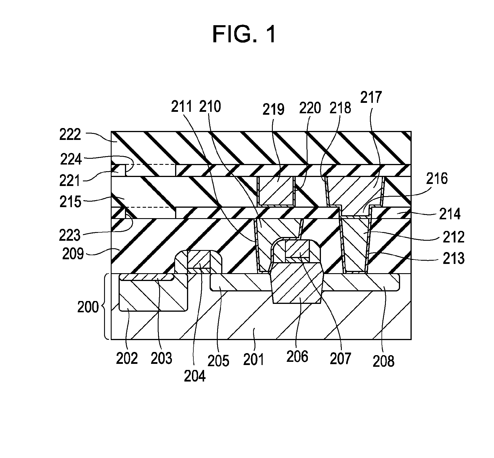
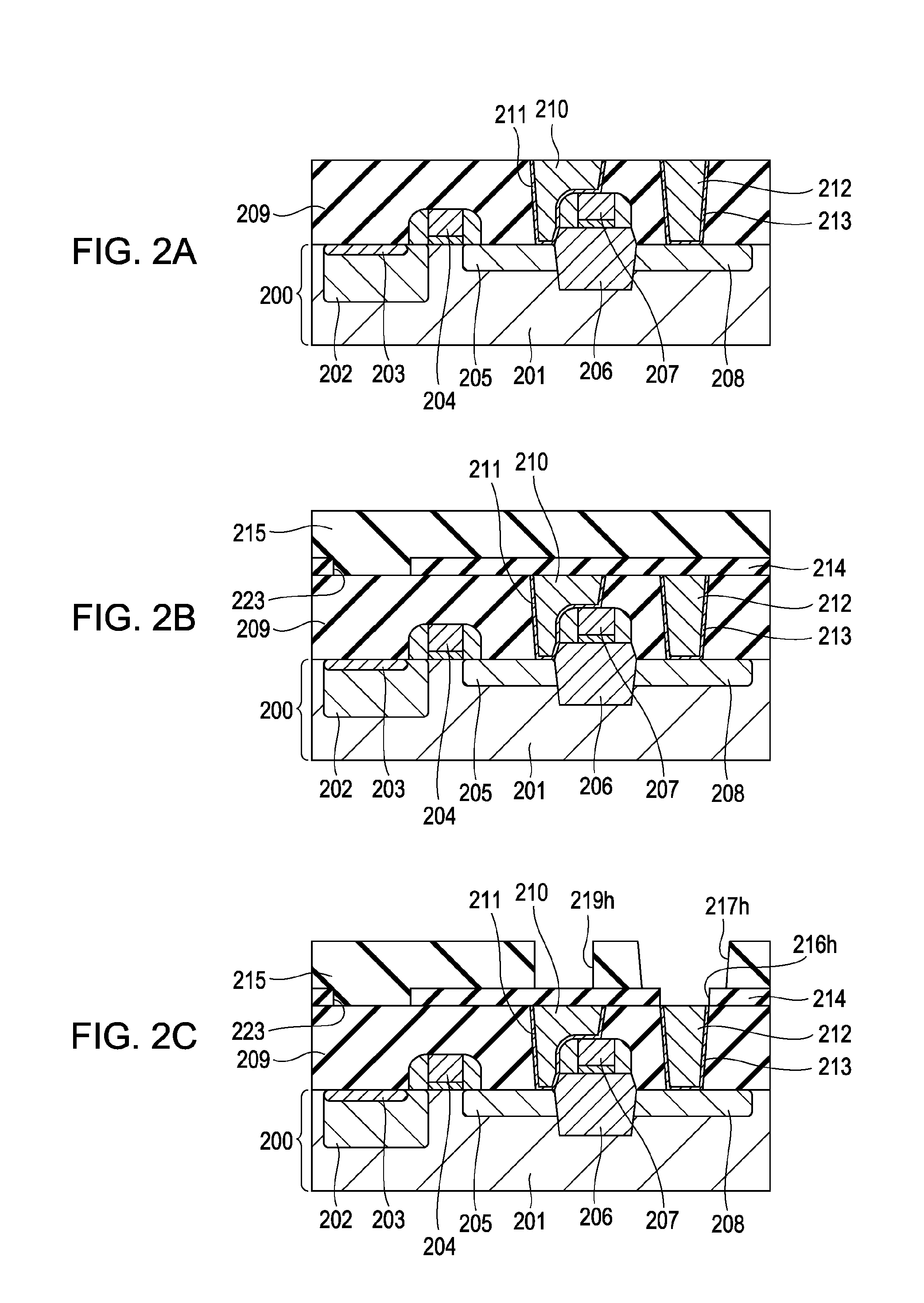
[0026]A first embodiment of the present invention is described with reference to FIG. 1. FIG. 1 is a cross-sectional schematic diagram of a pixel portion of a photoelectric conversion device and corresponds to a cross-section taken along a photoelectric conversion element 101 and a transferring MOS transistor 102 in FIG. 4.

[0027]Referring to FIG. 1, a semiconductor region 201 of a first conductivity type is formed in one main surface of a substrate 200. The first-conductivity-type semiconductor region 201 may be a well or the substrate itself. The substrate 200 also has a second-conductivity-type semiconductor region 202 and a first-conductivity-type region 203 covering the second-conductivity-type semiconductor region 202. A photoelectric conversion element is constituted by the first-conductivity-type semiconductor regions 201 and 203 and the second-conductivity-type semiconductor region 202. A gate electrode 204 of a transferring MOS transistor is provided to transfer charges of ...

second embodiment

Application to Imaging System

[0042]In a second embodiment, an example in which the photoelectric conversion device of the first embodiment is applied to an imaging system is described with reference to FIG. 5. An “imaging system” is a digital still camera, a digital video camera, a cellular phone digital camera, or the like.

[0043]FIG. 5 is a diagram showing the structure of a digital still camera. An optical image of a subject is focused on an imaging plane of a photoelectric conversion device 804 by an optical system including a lens 802 and the like. A barrier 801 that serves as a protector for the lens 802 and a main switch can be formed at the outer side of the lens 802. The lens 802 can be provided with a diaphragm 803 for controlling the quantity of light emitted from the lens 802. Imaging signals output via multiple channels from the photoelectric conversion device 804 are subjected to various processes such as correction and clamping in an imaging signal processing circuit 8...


PUM


Abstract

A photoelectric conversion device includes a semiconductor substrate, a first insulating film on the semiconductor substrate, a second insulating film on the first insulating film, a third insulating film on the second insulating film, and a wiring disposed in the third insulating film, the wiring being a wiring layer closest to the semiconductor substrate. A first plug of a shared contact structure and a second plug are disposed in the first insulating film. A third plug and a first wiring that constitute a dual damascene structure are disposed in the second and third insulating films. The first insulating film is used as an etching stopper film during etching of the second insulating film and the second insulating film is used as an etching stopper film during etching of the third insulating film.

Description

BACKGROUND OF THE INVENTION[0001]1. Field of the Invention[0002]The present invention relates to a photoelectric conversion device having a dual damascene structure and a method for making the photoelectric conversion device.[0003]2. Description of the Related Art[0004]Recently, high image quality, reasonably priced digital cameras and video cameras are gaining popularity. These image-input appliances are equipped with charge-coupled device (CCD)-type or metal oxide semiconductor (MOS)-type photoelectric conversion devices. A MOS photoelectric conversion device is constituted by a photoelectric conversion element, a MOS transistor, and other associated components. A MOS transistor can be formed by a complementary MOS (CMOS) process for general semiconductors.[0005]A MOS-type photoelectric conversion device uses a multilayer interconnection structure. Japanese Patent Laid-Open No. 2004-221527 discloses use of copper as a wiring material to decrease the thickness of the wiring and the...

Claims


Application Information

Patent Timeline
Patent Type & Authority Applications(United States)
IPC IPC(8): H04N5/335H01L31/18H01L31/14H01L27/14H01L27/146
CPCH01L27/14609H01L27/14689H01L27/14687H01L27/14636
Inventor AOKI, TAKESHISAWAYAMA, TADASHI
Owner CANON KK
Why Eureka
Try Eureka