Transparent type liquid crystal display device

a liquid crystal display and transparent technology, applied in non-linear optics, instruments, optics, etc., can solve the problem of increased pinhole defect produced in the electrode film covering the contact hole, and achieve the effect of suppressing the pinhole defect produced

Active Publication Date: 2010-04-01
PANASONIC LIQUID CRYSTAL DISPLAY CO LTD +1
View PDF3 Cites 10 Cited by
  • Summary
  • Abstract
  • Description
  • Claims
  • Application Information

AI Technical Summary

Benefits of technology

[0017]According to the invention, the bottom of the contact hole is covered with a transparent electrode film of two layers which ar

Problems solved by technology

This causes a problem that pinhole defect produced in th

Method used


Image

  • Transparent type liquid crystal display device
  • Transparent type liquid crystal display device
  • Transparent type liquid crystal display device

Examples


Embodiment Construction

[0033]Hereinafter, an embodiment of the invention will be described in detail based on the drawings.

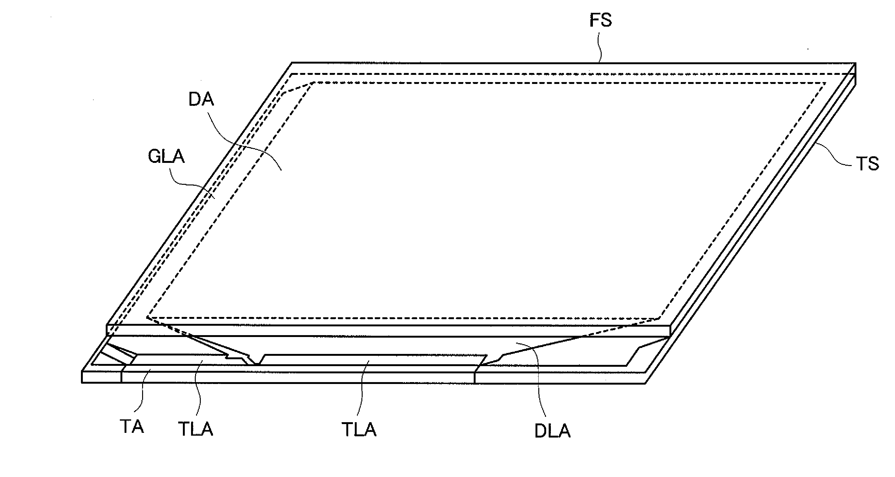
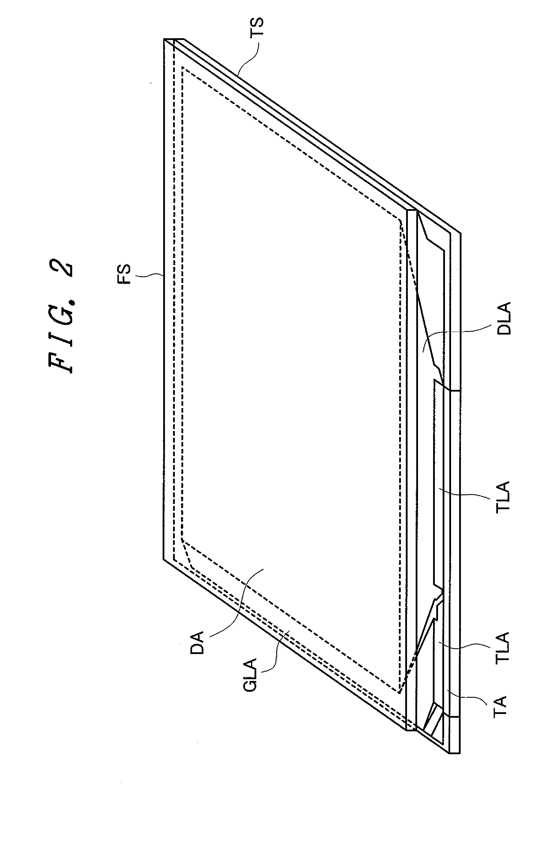
[0034]A transparent type liquid crystal display device according to the embodiment is a transparent type liquid crystal display device of an IPS system, including an array substrate TS, a filter substrate (counter substrate) FS which faces the array substrate TS and at which color filters are disposed, a liquid crystal material encapsulated in a region interposed between the two substrates, and a driver IC attached to the array substrate TS. Both of the array substrate TS and the filter substrate FS are glass substrates or the like.

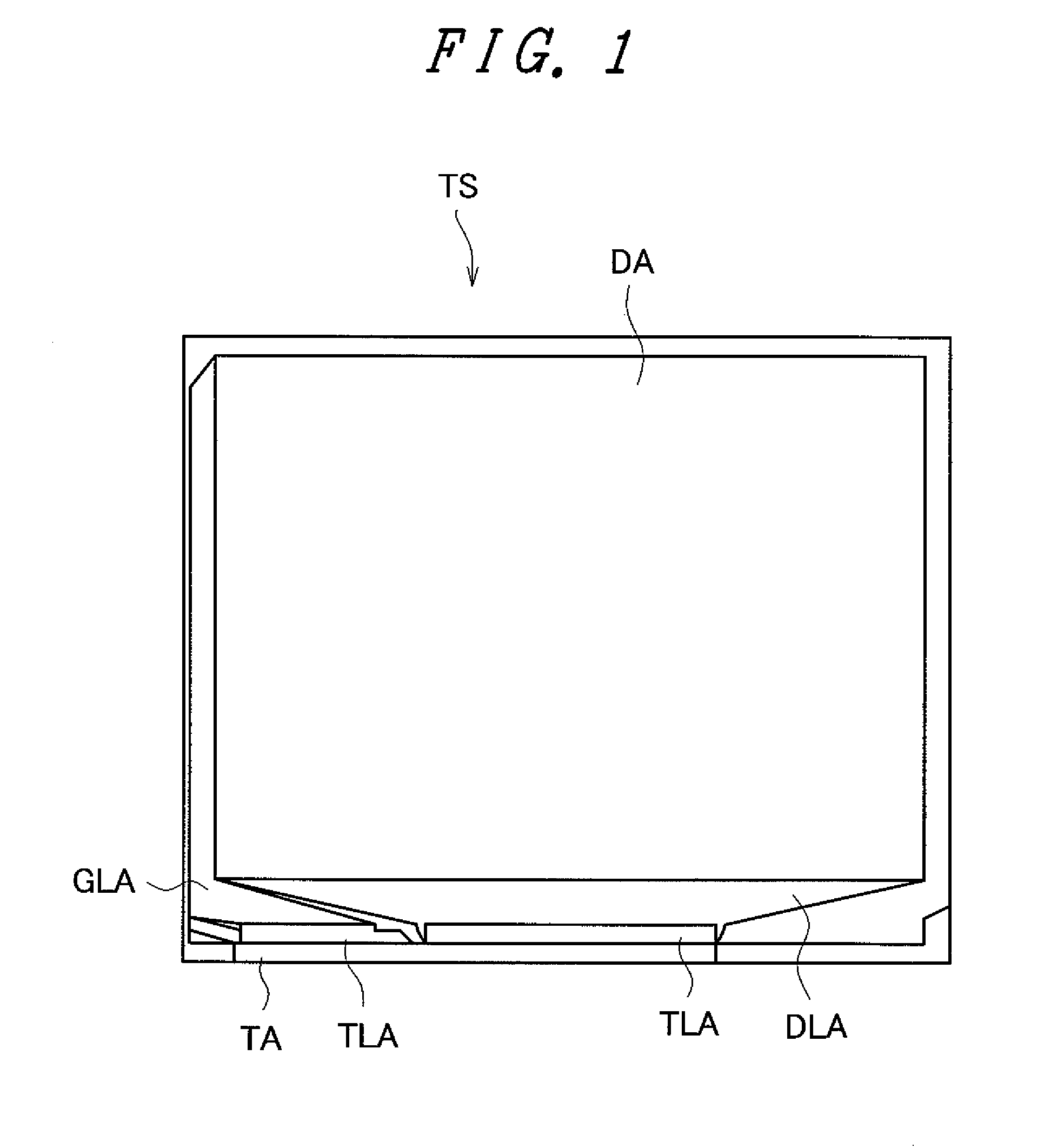
[0035]FIG. 1 is a plan view showing the layout of the array substrate TS according to the embodiment of the invention. At the array substrate TS, a display region DA in which numerous pixel circuits for displaying an image are arranged, a gate line routing region GLA which is adjacently disposed on the left side of the display region DA, a drain line routin...


PUM


Abstract

A first conductive layer in which a first electrode film is formed, a first protective layer on the first conductive layer, a first hole penetrating through the first protective layer to reach the first electrode film, a second conductive layer including a second electrode film which is disposed on the first protective layer and in contact with a portion of the first electrode film at the bottom of the first hole and the lower electrode, a second protective layer disposed on the second conductive layer and including the insulating film, a second hole disposed on the second protective layer and penetrating through the second protective layer to reach the second electrode film, and a third conductive layer including a third electrode film which is in contact with a portion of the second electrode film at the bottom of the second hole and the upper electrode.

Description

[0001]The present application claims priority from Japanese application JP2008-248955 filed on Sep. 26, 2008, the content of which is hereby incorporated by reference into this application.BACKGROUND OF THE INVENTION[0002]1. Field of the Invention[0003]The present invention relates to a transparent type liquid crystal display device.[0004]2. Background Art[0005]For example, a transparent type liquid crystal display panel of an IPS system is configured such that liquid crystal is retained between an array substrate at which a thin film transistor and the like are formed and a filter substrate (counter substrate) which faces the array substrate and at which color filters and the like are formed. A region of the array substrate corresponding to the display region of the liquid crystal display panel (hereinafter referred to as the display region of the array substrate) exists inside an encapsulated region where the liquid crystal is retained. A terminal portion of the array substrate fo...

Claims


Application Information

Patent Timeline
IPC IPC(8): G02F1/1343
CPCG02F1/134363G02F2001/13629G02F1/136227G02F1/13629
Inventor ASUMA, HIROAKIKITAJIMA, KENJIKAMADA, TAKAMITSUEDO, SUSUMUSUZUKI, RYOUHEI
Owner PANASONIC LIQUID CRYSTAL DISPLAY CO LTD
Why Eureka
Try Eureka