Normally emitting pixel architecture for frustrated total internal reflection displays

a technology of total internal reflection and pixel architecture, applied in the field of displays, can solve the problems of reducing the effective signal-to-noise ratio (and thus the contrast ratio) of the display system, compromising the efficiency of optical efficiency, and lifting the noise floor

Inactive Publication Date: 2010-04-01
RAMBUS DELAWARE
View PDF13 Cites 66 Cited by
  • Summary
  • Abstract
  • Description
  • Claims
  • Application Information

AI Technical Summary

Benefits of technology

[0020]In one embodiment, an apparatus is provided that includes a slab waveguide and one or more pixels deployed adjacent the top surface of the slab waveguide. In one embodiment, the slab waveguide is configured so that injected light is totally internally reflected at a top surface and a bottom surface of the slab waveguide. Each pixel includes a deformable active layer and a driver electronics layer. In a quiescent pixel state, the active layer is positioned adjacent and parallel to the top surface of the waveguide. The driver electronics layer is deployed in spaced-apart relationship to the active layer and opposite the slab

Problems solved by technology

For example, optical efficiency can be compromised because AM-TFT structures generally include a series of dielectric layers composed of several different materials suited to insure proper operation of the transistors.
In addition, the various layers of TFTs 114 and conductive interconnects 116 that may have canted surfaces with respect to the slab waveguide surface 133 and with respect to th

Method used


Image

  • Normally emitting pixel architecture for frustrated total internal reflection displays
  • Normally emitting pixel architecture for frustrated total internal reflection displays
  • Normally emitting pixel architecture for frustrated total internal reflection displays

Examples


Embodiment Construction

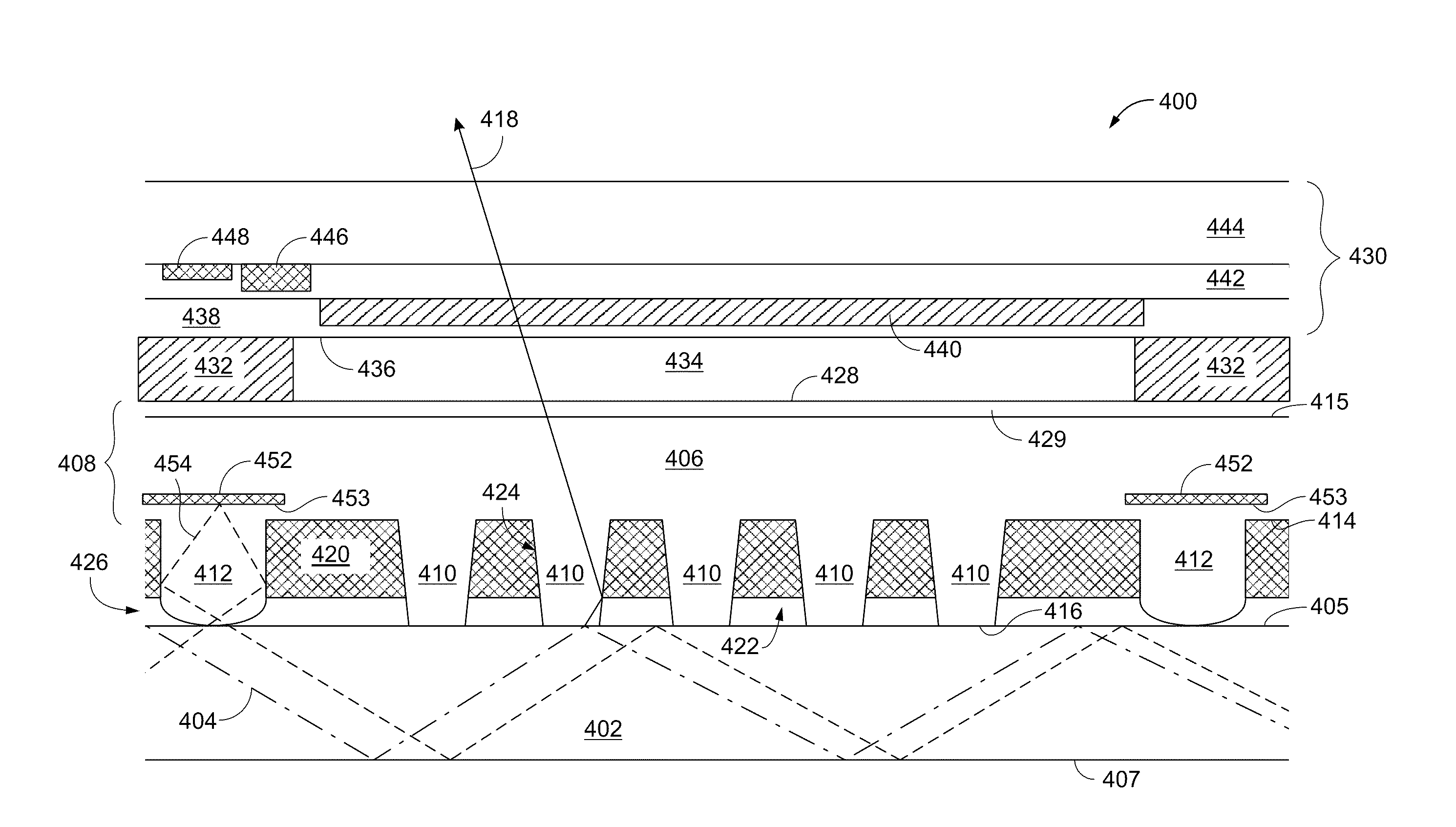
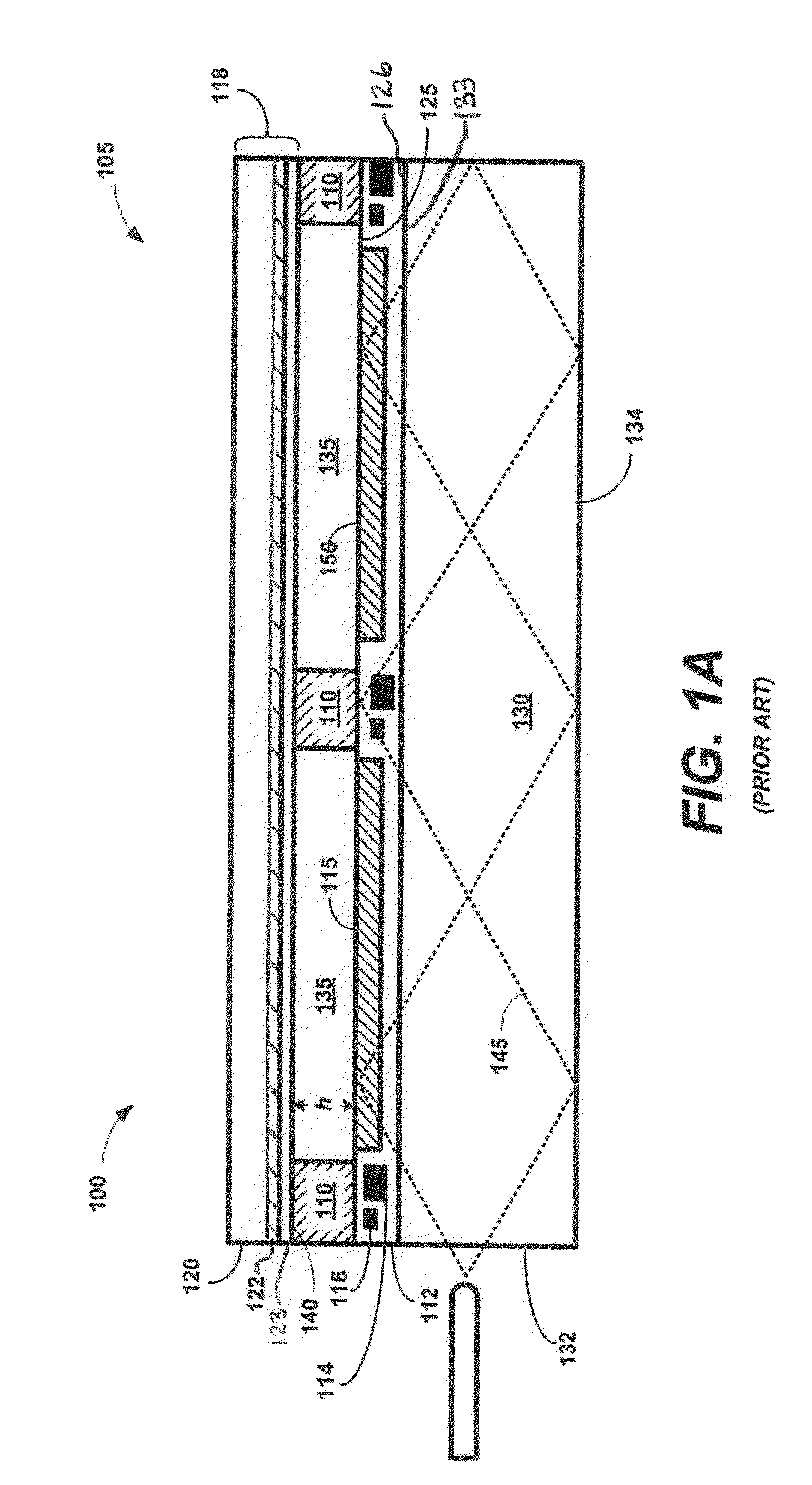
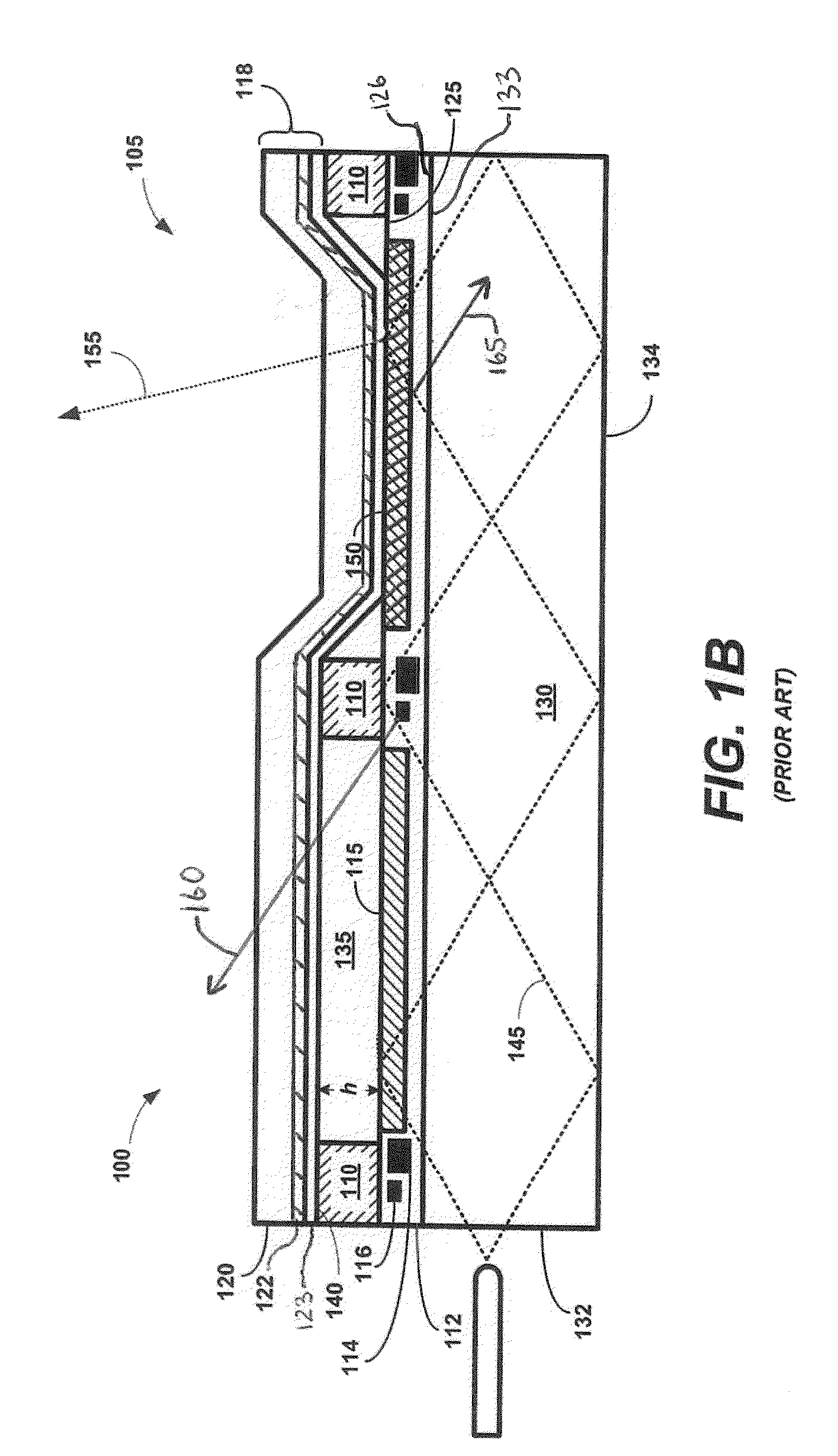
[0040]In the following description, illustrative embodiments are described to provide an understanding of the present invention. However, in the interest of clarity, not all features of an actual implementation are described in this specification. It will of course be appreciated that in the development of any such actual embodiment, numerous implementation-specific decisions should be made to achieve the developers' specific goals, such as compliance with system-related and business-related constraints, which will vary from one implementation to another. Moreover, it will be appreciated that such a development effort might be complex and time-consuming, but would nevertheless be a routine undertaking for those of ordinary skill in the art having the benefit of this disclosure.

[0041]The disclosed subject matter will now be described with reference to the attached figures. Various structures, systems and devices are schematically depicted in the drawings for purposes of explanation o...


PUM


Abstract

The present invention provides an apparatus that includes a waveguide and one or more pixels deployed adjacent the top surface of the waveguide which contains TIR light therein. Each pixel includes a deformable active layer having a first conductor and a driver electronics layer having a second conductor. The driver electronics layer is deployed in spaced-apart relation to the active layer and opposite the waveguide. In a quiescent state of a pixel, the active layer is in contact or near contact with the top surface of the waveguide so as to optically couple light out via FTIR (i.e., pixel's ON state). To actuate the pixel, the electronics layer is configured to selectively apply an electrical potential difference to the second conductor thereby causing the active layer to move away from the top surface so as to prevent the optical coupling of light out of the waveguide (i.e., pixel's OFF state).

Description

[0001]The earlier effective filing date of U.S. Provisional Application Ser. No. 61 / 091,176 filed Aug. 22, 2008 is hereby claimed under 35 U.S.C. §119. This provisional application is also hereby incorporated by reference for all purposes as if set forth verbatim herein.BACKGROUND OF THE INVENTION[0002]1. Field of the Invention[0003]This invention relates generally to the field of displays, and more particularly to enhancing the visual performance of transmissive displays that utilize a transparent slab waveguide to provide light to the pixel shuttering mechanisms that perform image modulation on the display surface.[0004]2. Description of the Related Art[0005]This section is intended to introduce the reader to various aspects of art that may be related to aspects of the present invention, which are described and / or claimed below. This discussion is believed to be helpful in providing the reader with background information to facilitate a better understanding of the present inventio...

Claims


Application Information

Patent Timeline
IPC IPC(8): G02F1/035
CPCG02B26/02G09F9/37G09G3/34
Inventor DERICHS, KEVIN J.KING, CAREYVAN OSTRAND, DANIEL K.COX, BERRY TODKILLION, REED J.
Owner RAMBUS DELAWARE
Why Eureka
Try Eureka