Apparatus and methods for improved control of quiescent state of output transistors in a class AB amplifier

a technology of output transistor and quiescent state, which is applied in the field of amplifier biasing, can solve the problems of unsatisfactory accuracy difficult and complex task of precise control of output load transistor,

Inactive Publication Date: 2002-04-09
MACOM TECH SOLUTIONS HLDG INC
View PDF3 Cites 20 Cited by
  • Summary
  • Abstract
  • Description
  • Claims
  • Application Information

AI Technical Summary

Problems solved by technology

However, as amplifiers are often composed of at least two stages that are internally compensated, precise control of the output load transistors becomes a difficult and complex task.
Presently known techniques for accurately controlling output device quiescent current have thus far been unsatisfactory, in part due to the difficulty associated with appreciating and replicating the relevant operating parameters of the output devices in the context of replica devices.

Method used


Image

  • Apparatus and methods for improved control of quiescent state of output transistors in a class AB amplifier
  • Apparatus and methods for improved control of quiescent state of output transistors in a class AB amplifier
  • Apparatus and methods for improved control of quiescent state of output transistors in a class AB amplifier

Examples


Embodiment Construction

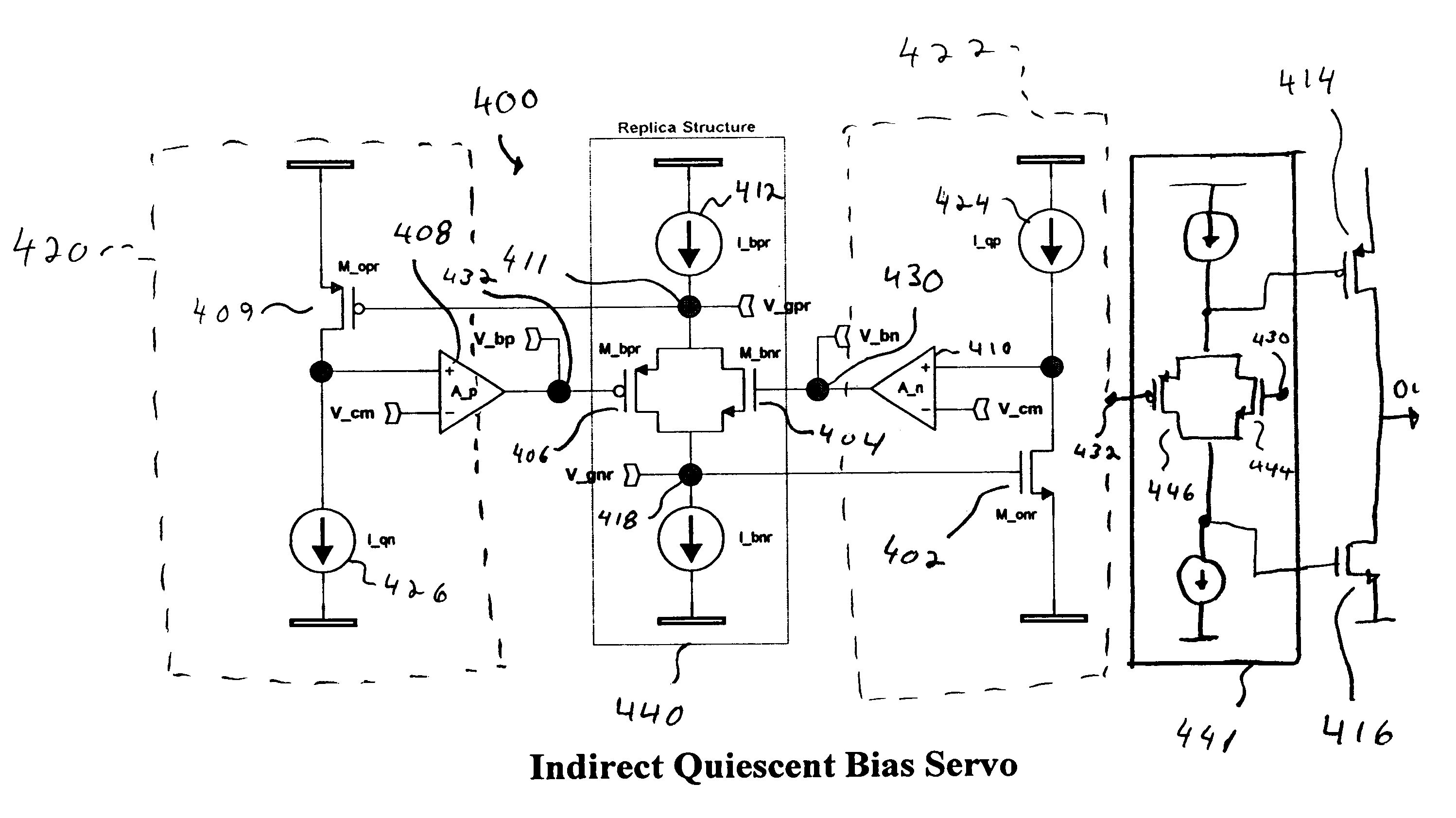
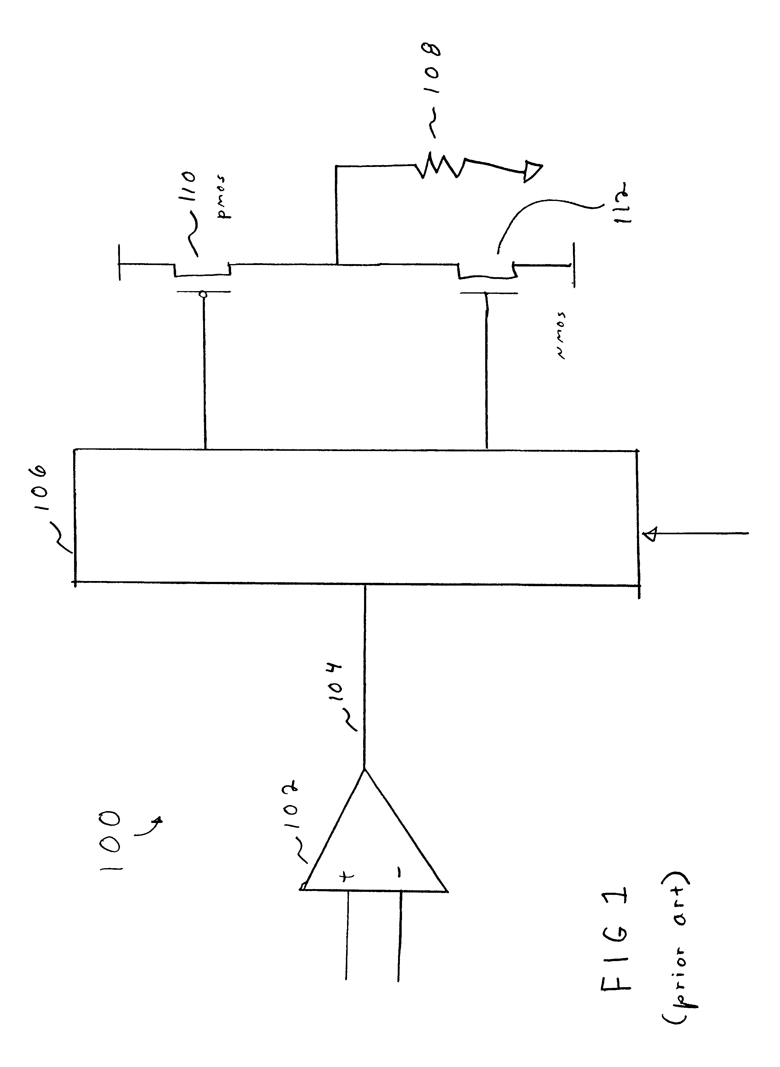
Referring now to FIG. 1, a block diagram of a typical prior art Class AB amplifier 100 suitably comprises a common source amplifier 102 having an output 104 applied through a coupler stage 106 to an output load 108. In the context of the present invention, output load 108 may be any device driven by a Class A, Class B, or Class AB amplifier, for example an audio speaker, a line driver for telecommunications equipment, or the like. Current is supplied to the output load 108 by a pair of complementary device transistors, namely, a PMOS or pull-up device transistor 110 and an NMOS or pull-down transistor 112. One of the principle functions of coupler circuit 106 is to precisely control the gate voltages to transistors 110 and 112, such that transistor 110 remains in the quiescent state while transistor 112 is pulled down, and such that transistor 112 is maintained in its quiescent state during the period in which transistor 110 is being pulled up.

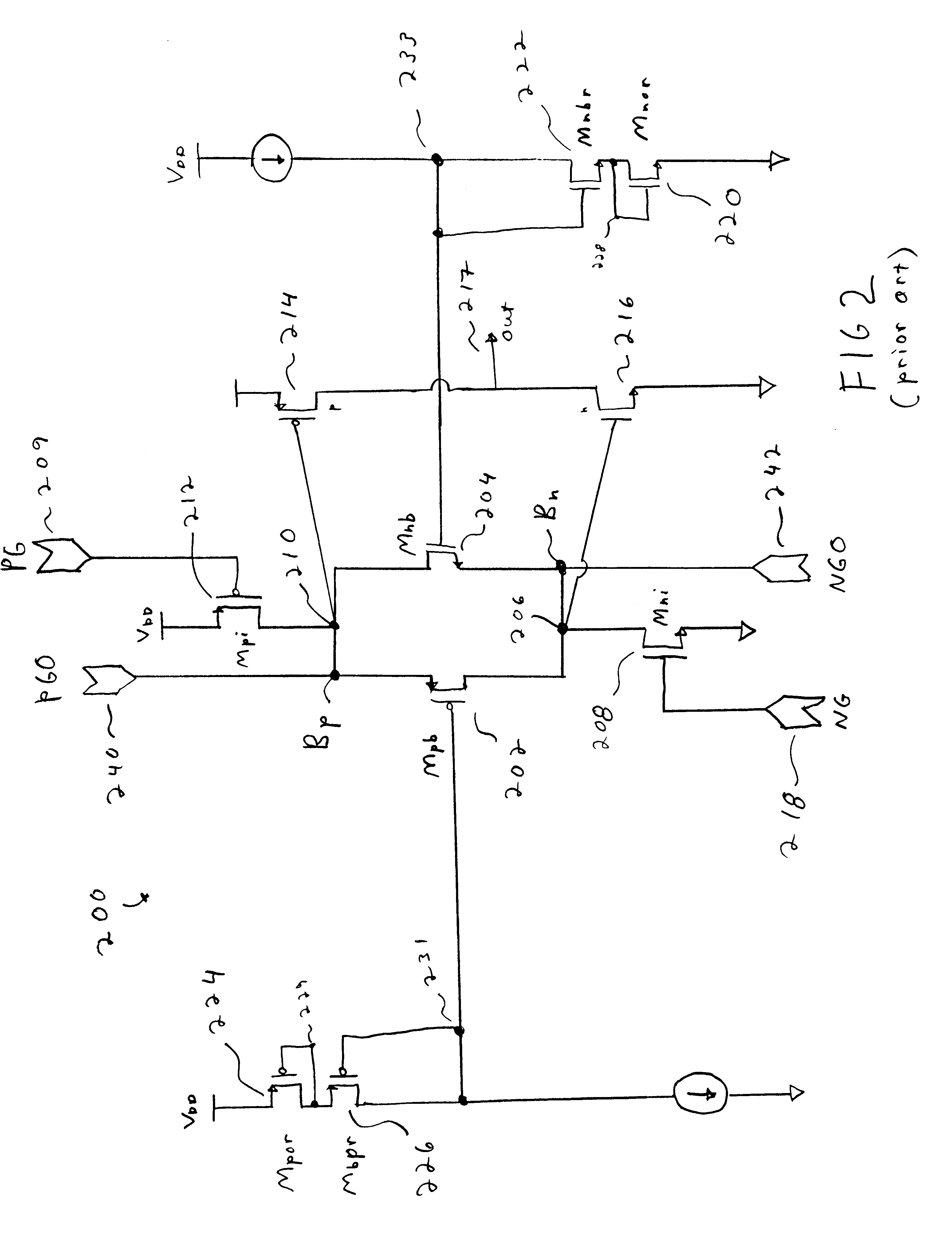
Referring now to FIG. 2, an exemplary p...


PUM


Abstract

A class AB amplifier biasing circuit is provided for controlling the quiescent state of a pull-up output device and a complimentary pull-down output device. The biasing circuit includes first and second current sources, each having a floating resistor configured to supply current to the pull-up and pull-down devices, respectively. The biasing circuit also includes gate control circuits for controlling the gate voltages of the first and second floating resistors. A device replica transistor is connected to a voltage node associated with the gate of the either the pull-up device or the pull-down device.

Description

1. Technical FieldThe present invention relates, generally, to amplifier biasing, and more particularly to circuit topologies for biasing an amplifier output stage for Class A, Class B or Class AB operation to achieve accurate quiescent control at the output stage, to thereby conserve power and maintain enhanced device linearity.2. Background Art and Technical ProblemsThe output stage of an amplifier provides a low output resistance that enables output signal delivery to a load with minimal loss of gain. While it is the primary function of the output stage to generate the output signal with minimal loss, it is also desirable to efficiently produce the output signal with minimal total harmonic distortion (THD). This implies that the power dissipated by the output stage is minimized, while providing suitable device linearity.In order to meet the various efficiency and linearity requirements for a given application, various biasing schemes have been proposed that are generally classifi...

Claims


Application Information

Patent Timeline
Patent Type & Authority Patents(United States)
IPC IPC(8): H03F3/30H03F1/30
CPCH03F1/308H03F3/3028H03F2200/453
Inventor KAPPES, MICHAEL S.
Owner MACOM TECH SOLUTIONS HLDG INC
Why Eureka
Try Eureka