Miniature and Multi-Band RF Coil Design

Active Publication Date: 2010-04-15
HONG KONG APPLIED SCI & TECH RES INST
19 Cites 82 Cited by

AI-Extracted Technical Summary

Problems solved by technology

The current path discontinuity adds some amount of capacitance to the RF coil, thereby affecting the frequency of operation, as well as...

Benefits of technology

[0009]The use of current path discontinuities and/or shorting bridges can enable an RF coil designer to create an RF coil that has an impedance that is already matched to a transmission line. Thus, some embodiments can eliminate external LC matching circuits such as circuit 1302 of FIG. 13. Furthermore, a current path discontinuity and/or a shorting bridge can be use...

Abstract

A near field apparatus comprises a Radio Frequency (RF) coil including at least one of a shorting bridge from a first point to a second point along an electrical path of the RF coil and/or a discontinuity in the electrical path of the RF coil.

Application Domain

Technology Topic

Image

  • Miniature and Multi-Band RF Coil Design
  • Miniature and Multi-Band RF Coil Design
  • Miniature and Multi-Band RF Coil Design

Examples

  • Experimental program(1)

Example

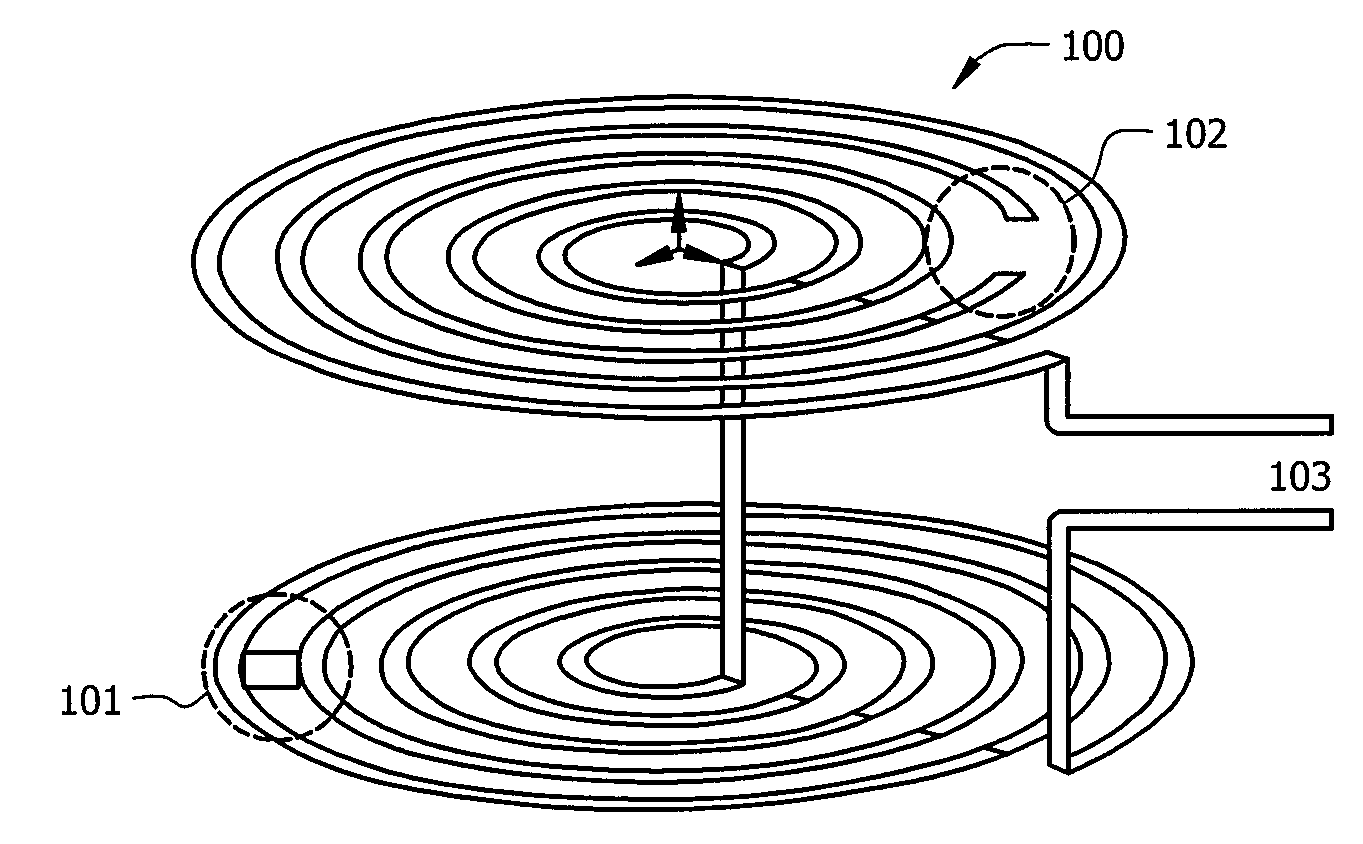
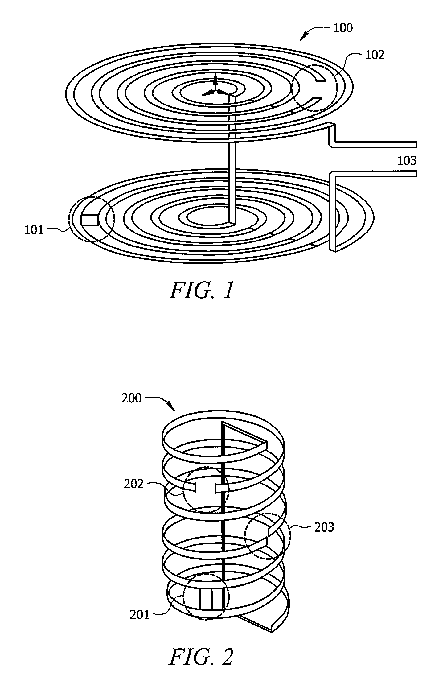
[0025]FIG. 1 is an illustration of exemplary RF coil 100 adapted according to one embodiment of the invention. RF coil 100 includes shorting bridge 101 and gap 102, which together affect the frequency performance of RF coil 100 as well as provide impedance matching at input/output port 103.
[0026]The scope of embodiments is not limited to the double-layer spiral type coil shown in FIG. 1. Embodiments of the invention can be adapted for use in any shape or type of RF coil, such as coils that include any number of layers, any number of turns, any sense of rotation in the turns, etc. For instance, FIG. 2 is an illustration of exemplary RF coil 200, adapted according to one embodiment of the invention. RF coil 200 is a helical type coil that includes shorting bridge 201 and gap 202 to provide impedance matching at input/output port 203 and frequency shifting.
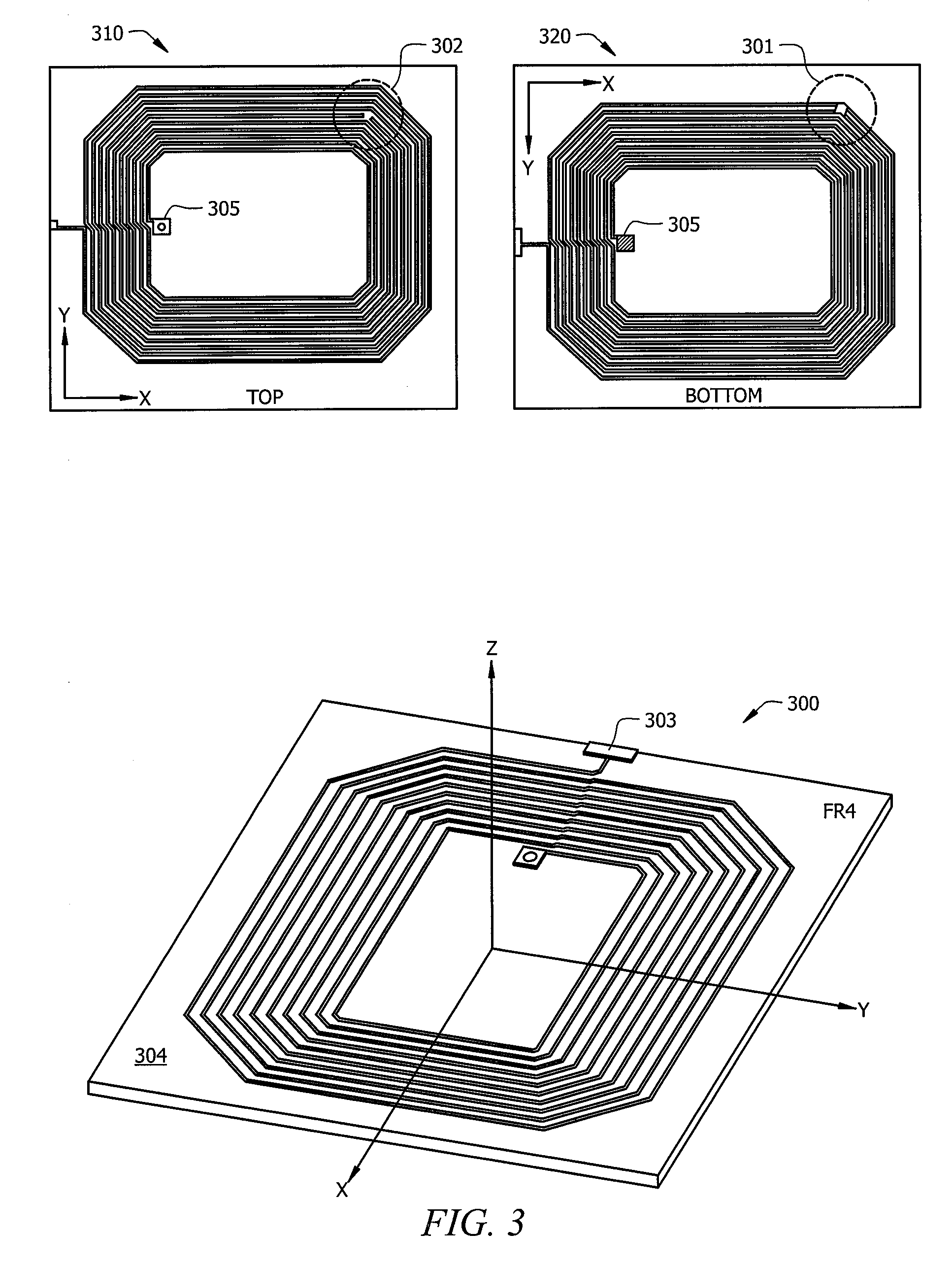
[0027]Nor is the scope of embodiments limited to coils that have both a gap and a shorting bridge, as some embodiments include either a gap or a shorting bridge. In fact some embodiments include two or more shorting bridges and/or gaps. The number of gaps and shorting bridges can be adapted for any given RF coil application.
[0028]RF coils adapted according to embodiments of the invention can be used in any application that transmits or detects energy in the near field. For example, embodiments of the invention can be used in RFID tags and readers, NFC cards and readers, MRI devices, and the like.
[0029]FIG. 3 is an illustration of exemplary RF coil 300, adapted according to one embodiment of the invention. RF coil 300 is topologically similar to RF coil 100 (FIG. 1) in that it is a double-layer spiral coil. RF coil 300 is disposed upon Printed Circuit Board (PCB) 304 with one layer on a top surface of PCB 304 (as shown in view 310) and another layer on a bottom surface of PCB 304 (as shown in view 320). Via 305 connects the two layers by providing a conductive path through PCB 304. RF coil 300 includes input/output port 303, thereby allowing RF coil 300 to be coupled to supporting components, such as a transmission line (not shown), an RF transceiver (not shown), amplifiers, driving circuits, and/or the like. View 310 shows gap 302, which is a discontinuity in the current path of RF coil 300. View 320 shows shorting bridge 301, which connects two adjacent turns of the current path.
[0030]A working prototype of the embodiment of FIG. 3 has been built on a PCB where the overall physical dimensions of the form factor (including PCB) is 80×55 mm, which is a typical RFID smart card size. The operating frequency of the prototype is 13.56 MHz, such that the prototype coil can be used in an RFID tag or reader. FIG. 4 shows the frequency response of the prototype compared to a frequency response of a similar coil that does not have a gap or shorting bridge. Curve 401 shows the frequency response of the prototype (employing a gap and shorting bridge, as shown in FIG. 3). Curve 402 shows the frequency response of a similar coil that does not include a gap or shorting bridge. As can be seen, the prototype according to an embodiment of the invention experiences a frequency shift and split due to the addition of the gap and shorting bridge. Thus, the addition of the gap and shorting bridge provides performance in a lower frequency range (as well as in another higher frequency range) compared to the other design that does not have a gap or shorting bridge.
[0031]As shown in FIG. 4, the embodiment of FIG. 3 provides performance in a lower frequency band than a coil without a gap or a short, but with no increase in coil size. It is estimated that the coil of FIG. 3 occupies seventy percent less surface area than a coil of the same shape as that of the coil of FIG. 3, lacking a gap or a shorting bridge, and configured to operate in the 13.56 MHz frequency band. Thus, one advantage of some embodiments is that coils can be miniaturized. Furthermore, the frequency split can provide for multi-band performance in some embodiments.
[0032]The embodiment of FIG. 3 is shown on a PCB substrate (i.e., PCB 304). However, the scope of embodiments includes any of a variety of substrates, such as flexible PCB or films used in RFID tags, and even includes no substrate at all for some coils.
[0033]FIG. 5 is an illustration of exemplary RF coil 500 adapted according to one embodiment of the invention. RF coil 500 is a helical type coil that has eighteen turns above the input/output port 503 and eighteen turns below the input/output port. The dimensions are about 115 mm long with 60 mm in coil diameter. RF coil 500 includes shorting bridge 501 and gap 502.
[0034]RF coil 500 can find use in an MRI application. For instance, a body part such as a knee or a wrist, can be put inside coil 500, which transmits and detects near field energy. RF coil 500 can be scaled up or scaled down to cover other body parts, such as legs, arms, and torsos. Scaling can be accomplished by making the diameter of coil 500 either larger or smaller, such that as the diameter increases, the number of turns of coil 500 can be reduced without changing the frequency response.
[0035]FIG. 6 is an illustration of a frequency response of a working prototype of the embodiment of FIG. 5. A coil with the same dimensions as coil500 (FIG. 5), but without a gap or shorting bridge, has a frequency response shown by curve 602. By contrast, coil 500 has a frequency response shown by curve 601. Curve 601 shows that the addition of gap 502 and shorting bridge 501 in coil 500 splits and shifts the bands of operation, providing bands of operation at 11.74 MHz and 34.27 MHz.
[0036]It is estimated that coil 500 occupies ninety percent less volume than a similarly shaped coil, without gap 502 and shorting bridge 501, configured to operate at 12 MHz. Thus, space savings is an advantage of some embodiments of the invention.
[0037]FIG. 7 is an illustration of exemplary method 700 adapted according to one embodiment of the invention. Method 700 may be performed, for example, by a group of designers creating an RF coil according to embodiments herein.
[0038]In action 701, a shape, an operating frequency, and an impedance of the RF coil are discerned. Often, but not always, the shape, the impedance, and the operating frequency are dictated by the particular application for which the RF coil will be used. In such instances, discerning the shape, impedance, and operating frequency includes becoming familiar with the constraints imposed by the near field application that will use the RF coil. For instance, MRI machines typically use helical coils operating at predefined frequencies, and matching impedances of the coils are chosen to correspond to transmission lines in the supporting circuitry.
[0039]In action 702, the placement of one or more of a current path discontinuity and a shorting bridge are determined by performing one or more actions. For instance, some embodiments include making one or more computer simulations to arrive at a satisfactory placement of the gap and/or short. The first simulation can be based on a best guess, and subsequent iterations can modify the starting simulated model until desired behavior and properties are achieved. A best guess often includes placing a shorting bridge on one half of a simulation model and placing a current path gap on the other half of the model in about the same place to achieve somewhat symmetrical placement of the shorting bridge and gap.
[0040]Yet another approach employs building and testing prototypes. The first prototype can be based on a best guess, whereas subsequent prototypes modify the original design iteratively until a desired model is achieved. Other techniques combine simulation modeling and prototypes. However, the scope of embodiments is not limited to any particular technique for determining placements of current path discontinuities and/or shorting bridges.
[0041]In action 703 the RF coil is manufactured with the current path discontinuity and/or the shorting bridge configured according to the determined placement. Any appropriate manufacturing process is within the scope of embodiments. In action 704, the RF coil is disposed in a near field application, such as an MRI device, an RFID tag or reader, an NFC tag or reader, and/or the like. In one example, the RF coil is coupled to a transmission line (e.g., a coaxial line) and the line is coupled to an RF transceiver. The transceiver is further coupled to one or more processors providing signal transmission control and received signal processing/display. Various embodiments of the invention can be disposed in near field applications in the same manner as conventional RF coils (though with different matching/tuning circuits or no matching/tuning circuits). Furthermore, RF coils according to various embodiments of the present invention can be expected to perform similarly to prior art RF coils of the same operating frequency.
[0042]Method 700 is not limited to placement of both a gap and a shorting bridge. Embodiments may place a gap and/or a shorting bridge and may even place more than one of a gap and/or a shorting bridge (e.g., two gaps and three shorting bridges or two shorting bridges and no gaps). Generally, a gap adds capacitance to the RF coil while a shorting bridge adds inductance. Embodiments that include both a gap and a shorting bridge, in effect, add an LC component to the RF coil. This is in contrast to other RF coils that have external LC components and/or components loaded within the coil structure that include capacitors and inductors. Accordingly, one advantage of some embodiments is the elimination of those LC components and, correspondingly, reduced numbers of parts and manufacturing costs.
[0043]Furthermore, while method 700 is shown as a series of discrete steps, the scope of embodiments is not so limited. Embodiments can add, omit, modify, and/or rearrange the actions of method 700. For instance, action 702 can be modified to include manual mathematical calculation of the coil properties.
[0044]FIG. 8 is an illustration of exemplary RF coils 810, 820, and 830 adapted according to embodiments of the invention. FIG. 8 illustrates that shorting bridges, such as bridges 811, 821, and 831, can be configured in a variety of different ways. For instance, shorting bridge 821 links points in two adjacent turns of RF coil 820. Shorting bridge 811 links two points in non-adjacent turns. Shorting bridge 831 links a top half of RF coil 830 to a bottom half. The placement and length will generally affect the inductance provided by a shorting bridge. A shorting bridge can be placed anywhere in an RF coil to link two non-adjacent points if it provides desired behavior. Furthermore, the width and placement of a gap affects its capacitance, and embodiments of the invention can include a gap of any of a variety of widths or placements to provide desired behavior.
[0045]Moreover, the RF coils themselves can conform to any of a variety of designs. For example, in a spiral coil with an upper and lower half, the two halves can have the same or different rotation sense, and the number of turns in the upper and lower halves can be the same or different. FIG. 9 is an illustration of exemplary coil designs that can be used in various embodiments. For instance, coil 910 is commonly called a “butterfly” coil, and coil 920 can be referred to as a “flower” coil. Any of the coils in FIG. 9 can be used alone, with a gap and/or a shorting bridge, in various embodiments. Furthermore, the coils of FIG. 9 can be combined in three-dimensional (3D) structures, for instance, with coil 910 on top and coil 920 below it, all connected in a current path. Gaps and/or shorting bridges can be distributed among the parts of the 3D structure.
[0046]Further, in many embodiments, the connections of the two ends of the current paths can be inside or outside of a structure, as in FIG. 10, which illustrates exemplary coils 1010 and 1020 adapted according to embodiments of the invention. In RF coil 1010, the ends of the current path are connected inside, whereas in RF coil 1020, the ends of the current path are connected outside. Such distinction does not typically affect performance of an RF coil, though it can impact usability of the RF coil as it is applied to a near field application. For instance, for an MRI coil that fits around a body part, a designer may prefer to connect to two ends of the current path outside of the coil, since the body part will fit inside. Furthermore, input/output ports are often connected to the current path at the place where the two ends of the current path are connected, and it can sometimes be more convenient to place a port outside, rather than inside, a 3D structure.
[0047]FIG. 11 is an illustration of exemplary RF coil array 1100 adapted according to one embodiment of the invention. For a given array, such as array 1100, a gap and/or shorting bridge can be placed in a single coil only. Alternatively, each coil in the array may include a gap and/or a short. Still further, gaps and/or shorting bridges can be distributed in any desirable way amongst the coils in the array. For instance, in array 1100, coil 1101 includes a gap and a shorting bridge, but coils 1102 and 1103 do not include a gap or a shorting bridge. An example MRI system can use a coil array, such as array 1100, to cover the whole body instead of using one large loop.
[0048]FIG. 12 is an illustration of exemplary RF coil array 1200 adapted according to one embodiment of the invention. Array 1200 is an array of spiral type RF coils, and the principle is the same as that of array 1100. Array 1200 includes a gap in RF coil 1202 and a shorting bridge in RF coil 1201. While not shown here, different types of coils (e.g., helical and spiral) can be combined in any of a variety of arrays.
[0049]Various embodiments of the invention offer advantages over the prior art. As mentioned above, embodiments provide a way to produce near field radiation in a given frequency band with a smaller coil than prior art embodiments provide. Furthermore, some embodiments provide a technique for adding inductance and/or capacitance to a coil other than by an external LC circuit or direct loading the capacitor or inductor within the coil.
[0050]Moreover, it should be noted that embodiments of the invention that employ a current path gap are new and revolutionary. Conventional thinking holds that RF coils should have continuous current paths, and embodiments of the invention directly contradict this long-held belief.
[0051]Although the present invention and its advantages have been described in detail, it should be understood that various changes, substitutions and alterations can be made herein without departing from the spirit and scope of the invention as defined by the appended claims. Moreover, the scope of the present application is not intended to be limited to the particular embodiments of the process, machine, manufacture, composition of matter, means, methods and steps described in the specification. As one of ordinary skill in the art will readily appreciate from the disclosure of the present invention, processes, machines, manufacture, compositions of matter, means, methods, or steps, presently existing or later to be developed that perform substantially the same function or achieve substantially the same result as the corresponding embodiments described herein may be utilized according to the present invention. Accordingly, the appended claims are intended to include within their scope such processes, machines, manufacture, compositions of matter, means, methods, or steps.

PUM

PropertyMeasurementUnit
Flexibility
Current
Frequency
tensileMPa
Particle sizePa
strength10

Description & Claims & Application Information

We can also present the details of the Description, Claims and Application information to help users get a comprehensive understanding of the technical details of the patent, such as background art, summary of invention, brief description of drawings, description of embodiments, and other original content. On the other hand, users can also determine the specific scope of protection of the technology through the list of claims; as well as understand the changes in the life cycle of the technology with the presentation of the patent timeline. Login to view more.

Similar technology patents

Classification and recommendation of technical efficacy words

  • Long wavelength
  • Reduce volume

Light-responsive artificial nucleotide having photo-crosslinking ability

ActiveUS8481714B2Less concern for any damageLong wavelengthSugar derivativesLong wavelengthPhoto crosslinking
Owner:JAPAN SCI & TECH CORP

Photovoltaic junction for a solar cell

ActiveUS20130269760A1Reducing degree of shiftLong wavelengthSemiconductor/solid-state device manufacturingNanoopticsPhysicsStatic force
Owner:LUMENTUM OPERATIONS LLC

Fingerprint identification module and fingerprint identification device

ActiveCN108399390ALong wavelengthStrong diffraction abilityPrint image acquisitionWave troughOpto electronic
Owner:BOE TECH GRP CO LTD +1

Implant release mechanism

ActiveUS20080140178A1Reduce volumeReduce outer diameterStentsOcculdersDilatorStent
Owner:COOK MEDICAL TECH LLC

Flash storage chip and flash array storage system

ActiveUS20080052451A1Reduce volumeImprove data transmission rateMemory adressing/allocation/relocationData transmissionPCI Express
Owner:PHISON ELECTRONICS

Devices and methods for placement of partitions within a hollow body organ

InactiveUS20070167960A1Reduce volumeSuture equipmentsStapling toolsTissue acquisitionBody organs
Owner:ETHICON ENDO SURGERY INC
Why Eureka
Try Eureka