Light-emitting device having a patterned surface

a light-emitting device and patterned surface technology, which is applied in the direction of semiconductor devices, basic electric elements, electrical appliances, etc., can solve the problems of affecting the epitaxial quality, affecting the light extraction efficiency and heat dissipation efficiency, and difficulty in subsequently epitaxial growth

Active Publication Date: 2010-04-22
EPISTAR CORP
View PDF2 Cites 43 Cited by
  • Summary
  • Abstract
  • Description
  • Claims
  • Application Information

AI Technical Summary

Benefits of technology

[0009]The disclosure provides a light-emitting device having a patterned surface to achieve both epitaxial quality and light-extraction efficiency.

Problems solved by technology

It worsens both the light extraction efficiency and the heat dissipation problems.
Nevertheless, the pattern is usually formed deeper in order to compensate the light loss due to the parallel (unpatterned) region, but the high aspect ratio of the deeper pattern causes difficulty for subsequently epitaxial growth and adversely affects the epitaxial quality.
By this method, it is hard to control the roughened dimension, such as the depth or the width.
Moreover, the epitaxial quality is not good by growing an epitaxial layer on the randomly rough surface.

Method used


Image

  • Light-emitting device having a patterned surface
  • Light-emitting device having a patterned surface
  • Light-emitting device having a patterned surface

Examples


first embodiment

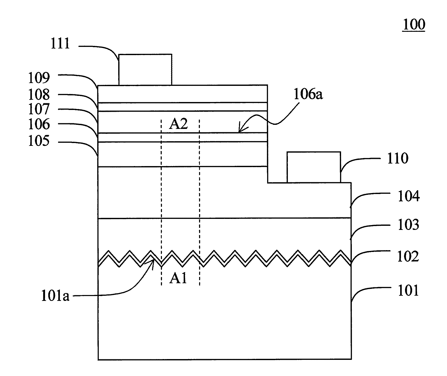
[0019]FIG. 1 shows a light-emitting device 100 in accordance with the present disclosure. The light-emitting device 100 comprises a growth substrate 101, an intermediate layer comprising a buffer layer 102 and / or an undoped semiconductor layer 103 epitaxially grown on the growth substrate 101, a first contact layer 104 with first conductivity-type epitaxially grown on the intermediate layer, a first cladding layer 105 with first conductivity-type epitaxially grown on the first contact layer 104, an active layer 106 epitaxially grown on the first cladding layer 105, a second cladding layer 107 with second conductivity-type epitaxially grown on the active layer 106, a second contact layer 108 with second conductivity-type epitaxially grown on the second cladding layer 107, a current spreading layer 109 formed on the second contact layer 108 and forming an ohmic contact with the second contact layer 108, a first electrode 110 formed on the exposed first contact layer 104 by evaporation...

second embodiment

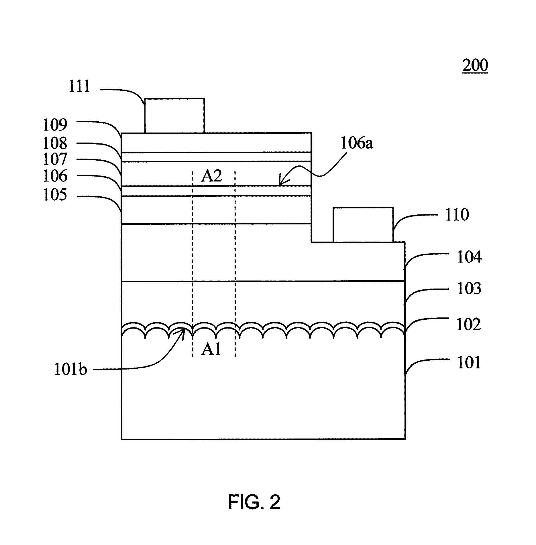
[0020]FIG. 2 shows a light-emitting device 200 in accordance with the present disclosure. In comparison with the light-emitting device 100 shown in FIG. 1, the cross-section of the patterned surface 101b comprises a plurality of ordered patterned units, and each of the patterned units comprises a smooth curve for facilitating the subsequently grown buffer layer 102 and / or the undoped semiconductor layer 103 to fill into the depressed area of the patterned surface 101b. The method for forming the cross-section with a smooth curve comprises firstly forming a mask layer of photoresist on a plane substrate, patterning the mask layer by lithographic process, then curing the patterned mask layer in a baking machine under an appropriate temperature to reflow the patterned mask layer of photoresist to form a profile with smooth curve, finally dry-etching or wet-etching the substrate with the patterned mask layer to transfer the smooth curve profile to the substrate to form a patterned surfa...

third embodiment

[0021]FIG. 3 shows a light-emitting device 300 in accordance with the present disclosure. In comparison with the light-emitting device 200 shown in FIG. 2, the patterned surface 101c of the light-emitting device 300 comprises a plurality of patterned units with variable dimensions or variable patterns disposed in a fixed period, variable period, or quasi-period. The top views of the plurality of the pattern units comprise polygon, or at least one pattern selected from the group consisting of triangle, rectangle, hexagon, and circle. The cross-section of the plurality of pattern units comprises at least two curves with different curvatures.


PUM


Abstract

The disclosure provides a light-emitting device comprising a substrate, an intermediate layer formed on the substrate, a first doped semiconductor layer with first conductivity-type formed on the intermediate layer, a second doped semiconductor layer with second conductivity-type formed on the first doped semiconductor layer, an active layer formed between the first doped semiconductor layer and the second doped semiconductor layer, and a patterned surface having a plurality of ordered pattern units; wherein the patterned surface is substantially not parallel to the corresponding region of the surface of the active layer.

Description

RELATED APPLICATION[0001]This application is a continuation-in-part of U.S. patent application Ser. No. 12 / 222,548, entitled “Stamp Having Nanoscale Structure And Applications Thereof In Light-Emitting Device”, filed on Aug. 12, 2008; and claims the right of priority based on TW application Ser. No. 097150633 filed on Dec. 24, 2008; the contents of which are incorporated herein by reference in their entirety.BACKGROUND[0002]1. Technical Field[0003]The present disclosure relates to a light-emitting device having a patterned surface.[0004]2. Description of the Related Art[0005]Recently, efforts have been devoted to promote the luminance of the light-emitting diode (LED) in order to implement the device in the lighting domain, and further procure the goal of energy conservation and carbon reduction. There are two major aspects to promote luminance. One is to increase the internal quantum efficiency (IQE) by improving the epitaxy quality to enhance the combination efficiency of electron...

Claims


Application Information

Patent Timeline
Patent Type & Authority Applications(United States)
IPC IPC(8): H01L33/00
CPCH01L33/22H01L33/24H01L2933/0091H01L33/20H01L33/12H01L33/30H01L33/32
Inventor OU, CHENYAO, CHIU-LIN
Owner EPISTAR CORP
Why Eureka
Try Eureka