Backside-illuminated solid-state image pickup device

a solid-state image and pickup device technology, applied in the direction of radio frequency controlled devices, television system scanning details, etc., can solve the problems of analog circuits that cannot produce stable waveforms, pulse noises are likely to leak in logic circuits, and the back surface of silicon substrates cannot be grounded with the back surface of silicon substrates bonded to a package, etc., to achieve stable waveforms and less nois

Inactive Publication Date: 2010-04-22
KK TOSHIBA
View PDF0 Cites 30 Cited by
  • Summary
  • Abstract
  • Description
  • Claims
  • Application Information

AI Technical Summary

Benefits of technology

[0014]The present invention can provide a backside-illuminated solid-state image pickup device capable of allo

Problems solved by technology

However, the backside-illuminated image pickup device has the following problem related to grounding.
In contrast, having the microlenses and the like on the backside of the silicon substrate, the backside-illuminated image pickup device cannot be grounded with the back surface of the silicon substrate bonded to a package.
However, this image pickup device is configured without consideratio

Method used


Image

  • Backside-illuminated solid-state image pickup device
  • Backside-illuminated solid-state image pickup device
  • Backside-illuminated solid-state image pickup device

Examples


first embodiment

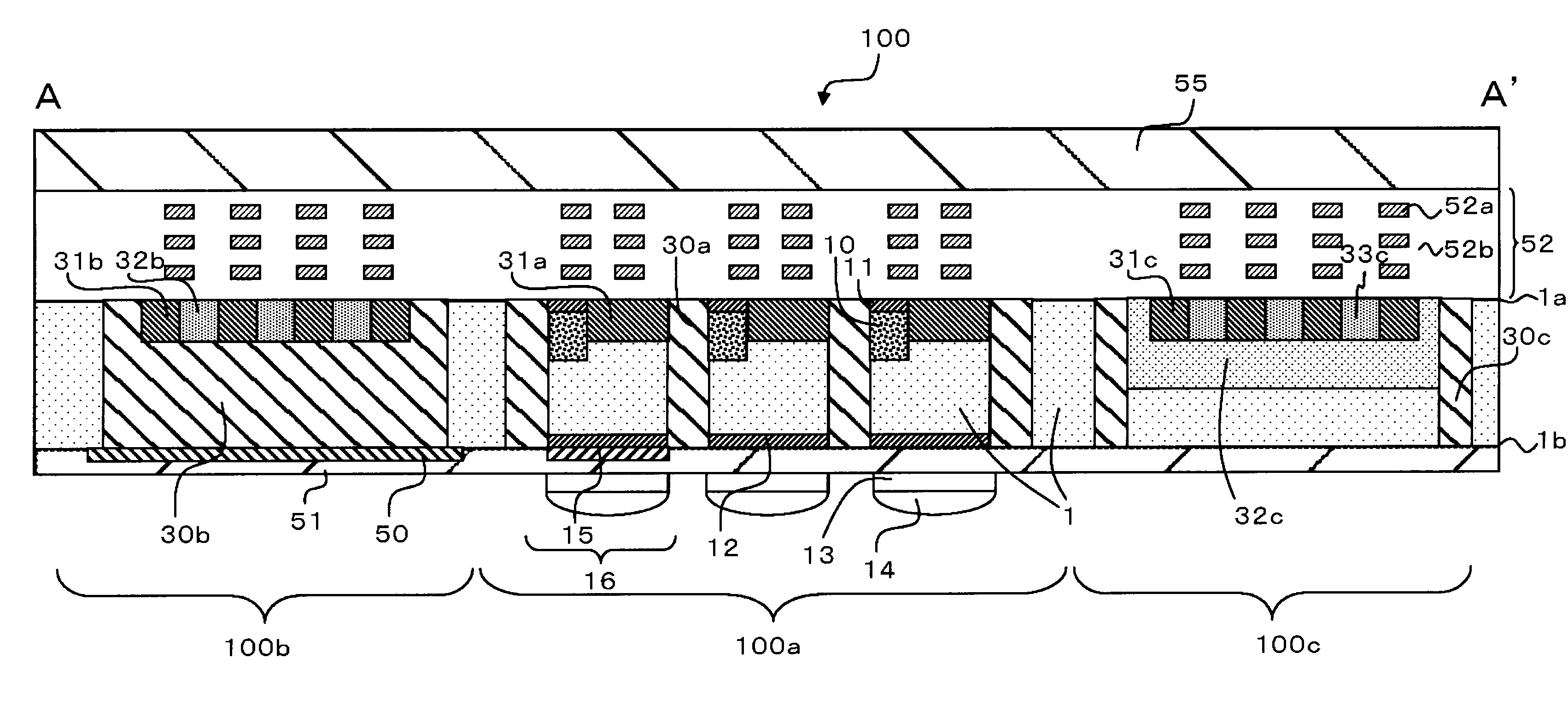
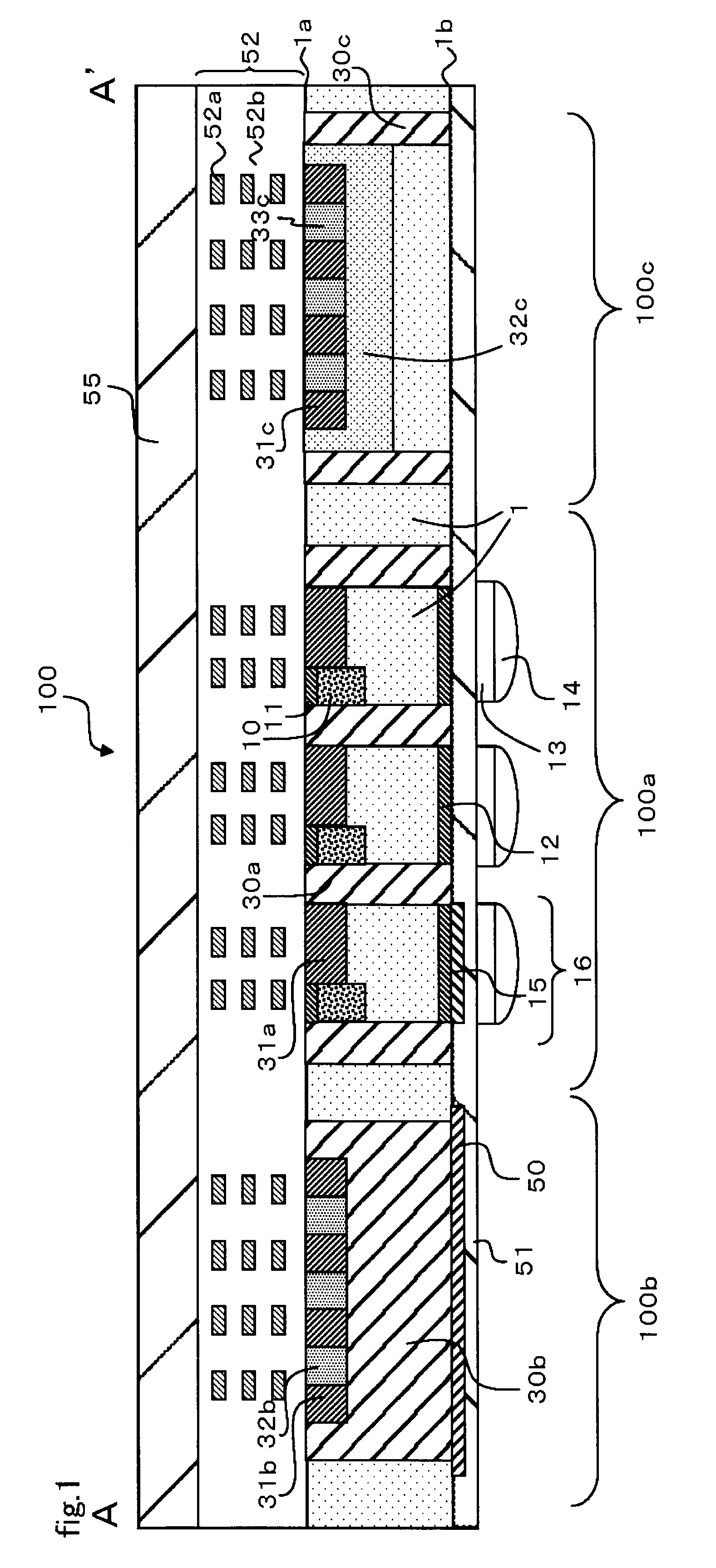
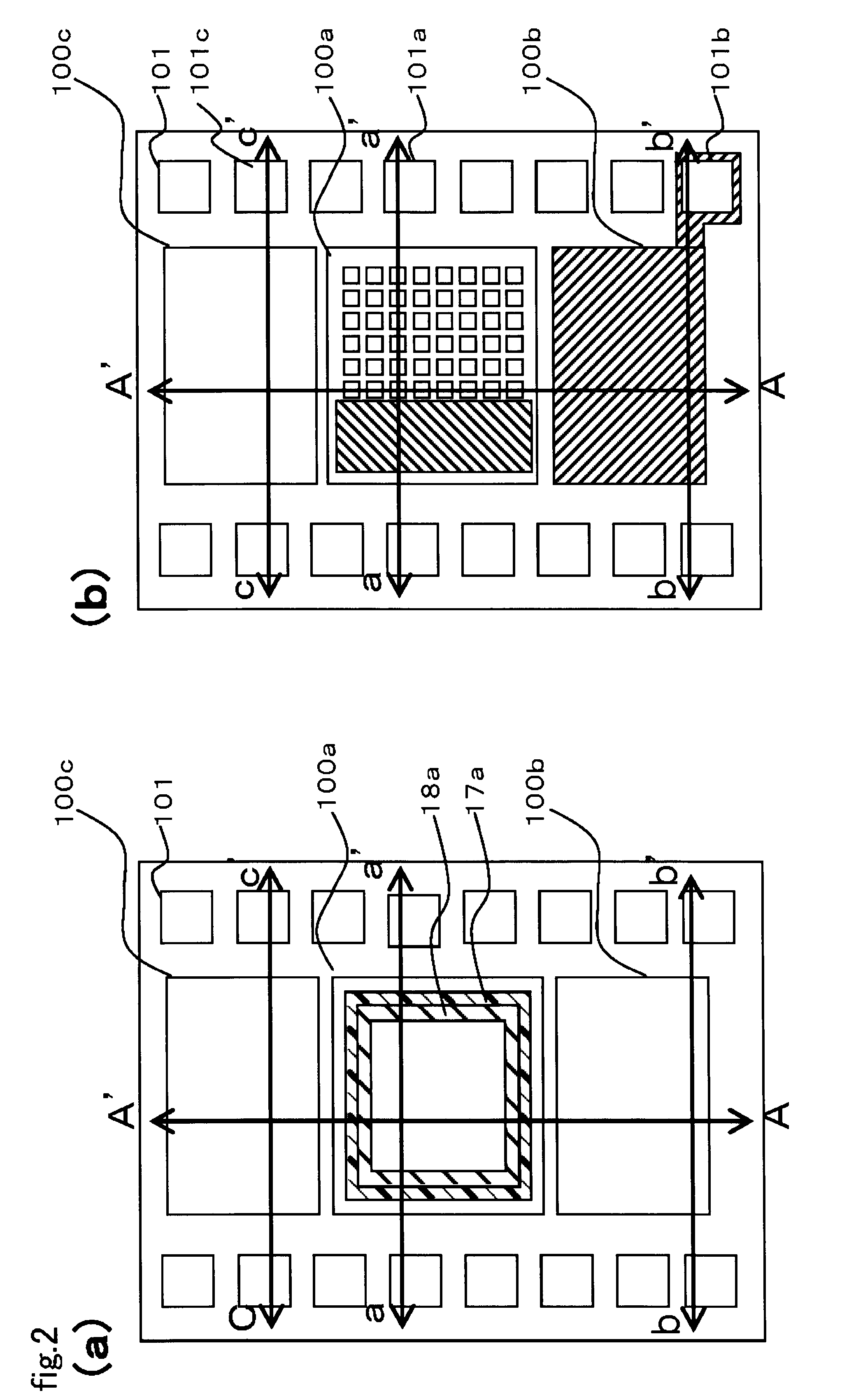
[0031]FIG. 1 is a cross-sectional view of a backside-illuminated solid-state image pickup device 100 according to a first embodiment of the present invention, and FIGS. 2A and 2B are plan views of the backside-illuminated solid-state image pickup device 100 according to the first embodiment of the present invention (in which FIG. 2A shows a front surface side and FIG. 2B shows a back surface side). Note that the cross-sectional view in FIG. 1 is one taken along an A-A′ line in FIG. 2.

[0032]As shown in FIG. 1, the backside-illuminated solid-state image pickup device 100 of this embodiment includes an N type semiconductor layer 1, and this semiconductor layer 1 includes a first principal surface (a front surface) 1a and a second principal surface (a back surface) 1b opposed to this first principal surface 1a. Moreover, this semiconductor layer 1 includes a pixel area 100a, and an analog circuit area 100b as well as a logic circuit area 100c which collectively serve as a peripheral cir...

second embodiment

[0074]FIG. 11 is a cross-sectional view of a backside-illuminated solid-state image pickup device 100 according to a second embodiment of the present invention, and FIGS. 12A and 12B are plan views of the backside-illuminated solid-state image pickup device 100 according to the second embodiment of the present invention (in which FIG. 2A shows a front surface side and FIG. 2B shows a back surface side). Note that the cross-sectional view in FIG. 11 is one taken along an A-A′ line in FIG. 12.

[0075]This embodiment is different from the first embodiment in that the metal layer which is grounded is provided only on the back surface side of the analog circuit area in the first embodiment, whereas metal layers which are grounded are also provided on the back surface side of the pixel area and the logic circuit area in this embodiment.

[0076]To be more precise, as shown in FIG. 11, the backside-illuminated solid-state image pickup device 100 of this embodiment also includes the metal layers...

third embodiment

[0090]FIG. 15A is a cross-sectional view of a backside-illuminated solid-state image pickup device 100 according to a third embodiment of the present invention, and FIG. 15B is a plan view of the backside-illuminated solid-state image pickup device 100 according to the third embodiment of the present invention.

[0091]This embodiment is different from the second embodiment in that a metal layer 50 which is grounded and has a film thickness of 300 to 800 nm is formed on the second principal surface 1b side of the logic circuit area 100c and of the analog circuit area 100b.

[0092]Specifically, the logic circuit area 100c includes the first P type area 30c formed to lie between the first principal surface 1a and the second principal surface 1b, the metal layer 50 formed at least partially on the second principal surface 1b of the first P type area 30c, the second N type area formed in part of the first principal surface 1a side of the first P type area 30c, and the VSS pad 101c electrica...


PUM


Abstract

Provided is a backside-illuminated solid-state image pickup device capable of allowing peripheral circuits to produce stable waveforms and thereby achieving image characteristics with less noise, the device including: a first-conductivity-type semiconductor layer having a first principal surface and a second principal surface opposed to the first principal surface and also having a pixel area and an analog circuit area; a first P type area formed to lie between the second principal surface and the first principal surface in the analog circuit area; a metal layer formed at least partially on the second principal surface of the first P type area; a VSS electrode electrically connected to the metal layer; a photo-conversion area formed in the pixel area and used to accumulate electric charges generated by photoelectric conversion; and a microlens provided on the second principal surface in the pixel area so as to correspond to the photo-conversion area.

Description

CROSS-REFERENCE TO RELATED APPLICATIONS[0001]This application is based upon and claims the benefit of priority from prior Japanese Patent Application No. P2008-269456, filed on Oct. 20, 2008; the entire contents of which are incorporated herein by reference.BACKGROUND OF THE INVENTION[0002]1. Field of the Invention[0003]The present invention relates to a backside-illuminated solid-state image pickup device and a manufacturing method thereof.[0004]2. Description of the Related Art[0005]The market for small-sized camera modules has been drawing attention in recent years with application of these modules to digital still cameras or camera-equipped mobile telephones. With a size reduction of pixels, an image device such as a CCD or a CMOS image sensor used for such a camera module may have lower sensitivity reduced due to a reduction in a photoelectric conversion area. The factors of the sensitivity reduction include the reduction in the photoelectric conversion area due to smaller pixe...

Claims


Application Information

Patent Timeline
IPC IPC(8): H01L31/112H01L31/0232H01L27/146
CPCH01L27/14623H01L27/1463H01L27/1464H01L2924/0002H01L2924/00
Inventor INOUE, IKUKO
Owner KK TOSHIBA
Why Eureka
Try Eureka