Liquid crystal display device, scan signal drive device, liquid crystal display device drive method, scan signal drive method, and television receiver

a liquid crystal display device and signal drive technology, applied in the direction of electric digital data processing, instruments, computing, etc., can solve the problems of deterioration of elements, drop in charging rate of pixel, and plus/minus voltage to be applied to liquid crystal

Inactive Publication Date: 2010-04-22
SHARP KK
View PDF29 Cites 32 Cited by
  • Summary
  • Abstract
  • Description
  • Claims
  • Application Information

AI Technical Summary

Benefits of technology

[0079]With the arrangement, it is possible to appropriately perform the aforementioned driving using relatively simple configurations of the flip-flop, the mask, and the OR logic operation section.
[0080]Further, it is possible to produce a television receiver including the liquid crystal display device of the present invention and a tuner section for receiving television broadcasting.

Problems solved by technology

If a current voltage continues to be applied to a liquid crystal layer of such liquid crystal display device for a long time, elements get deteriorated.
However, in a case where an active matrix liquid crystal display device employs frame inversion driving in which the polarity of a voltage is inverted with respect to each frame, it is inevitable that some unbalance is seen in a plus / minus voltage to be applied to liquid crystal due to anisotropy of liquid crystal dielectric constant, variation in pixel potential that is caused by parasitic capacitance between a gate and a source of a pixel TFT, and a slip of a center value of a counter electrode signal.
When dot inversion in which the polarity of a voltage is inverted with respect to each pixel is performed, a charging rate of a pixel drops due to signal delay in a data signal line.
However, this technique still raises a problem that a charging rate of a pixel drops at a row where the polarity of a data signal voltage is inverted.

Method used


Image

  • Liquid crystal display device, scan signal drive device, liquid crystal display device drive method, scan signal drive method, and television receiver
  • Liquid crystal display device, scan signal drive device, liquid crystal display device drive method, scan signal drive method, and television receiver
  • Liquid crystal display device, scan signal drive device, liquid crystal display device drive method, scan signal drive method, and television receiver

Examples


embodiment 1

[0295]One embodiment of the present invention is described below with reference to the attached drawings.

[0296](Structure of Liquid Crystal Display Device)

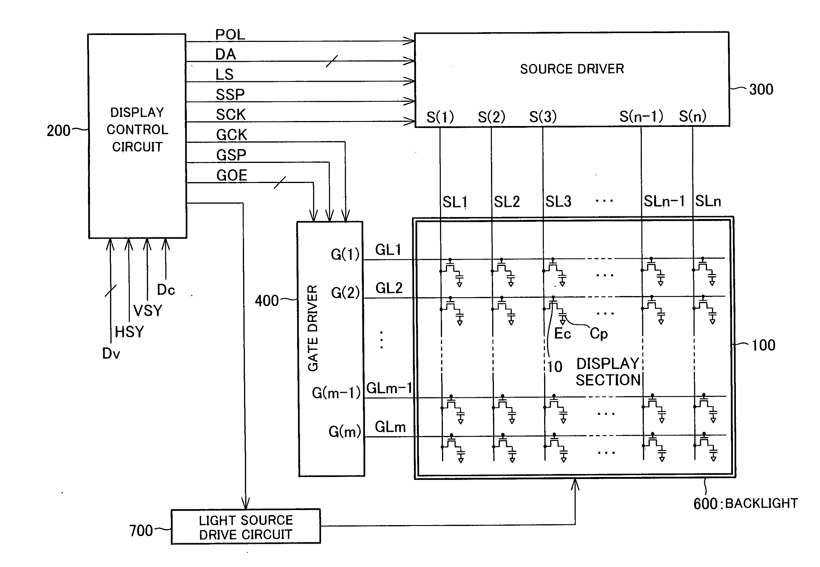
[0297]FIG. 1 is a block diagram showing a structure of a liquid crystal display device of the present invention and an equivalent circuit of a display section of the liquid crystal display device. The liquid crystal display device includes a source driver 300 serving as a data signal line drive circuit, a display section 100 that is an active matrix display section, a backlight 600 serving as a planer illuminating device, a light source drive circuit 700 for driving the backlight 600, and a display control circuit 200 for controlling the source driver 300, the gate driver 400, and the light source drive circuit 700. In the present embodiment, the display section 100 is an active matrix liquid crystal panel. Alternatively, the display section 100 may be integrated with the source driver 300 and the gate driver 400 to form a liquid ...

embodiment 2

[0368]Another embodiment of the present invention is described below with reference to the drawings. Configurations having the same functions as those in Embodiment 1 are given the same reference numerals and explanations thereof are omitted here.

[0369](Configuration of Liquid Crystal Display Device)

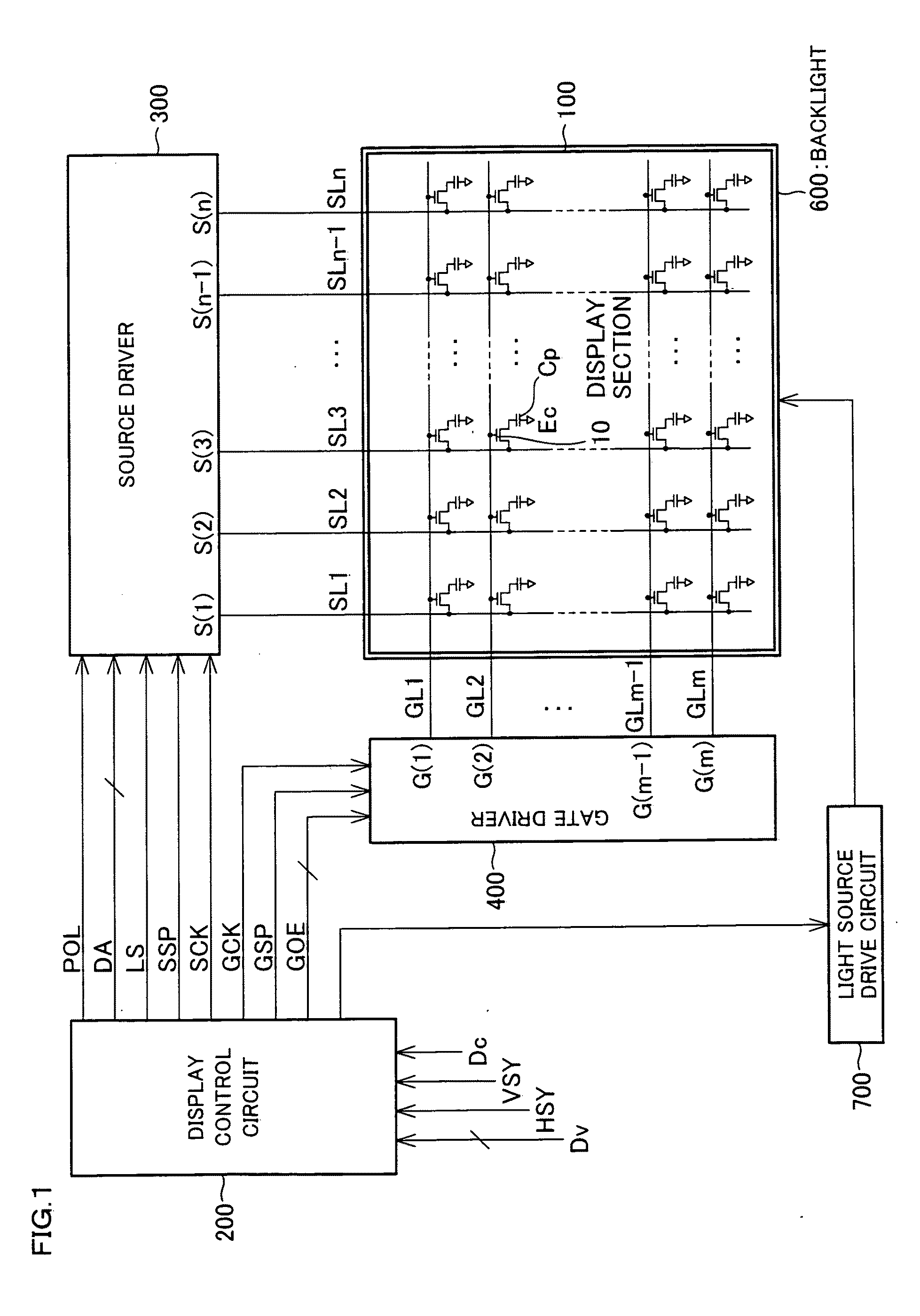
[0370]FIG. 15 is a block diagram illustrating a configuration of a liquid crystal display device of the present embodiment and an equivalent circuit of a display section of the liquid crystal display device. The liquid crystal display device is obtained by arranging the liquid crystal display device of FIG. 1 so as to further include a CS control circuit (retention capacitor signal drive section) 90 serving as an auxiliary capacitor line drive circuit. Except for the CS control circuit 90, the liquid crystal display device of the present embodiment is the same as the liquid crystal display device of Embodiment 1 and therefore explanation thereof is omitted here.

[0371]The CS control circu...


PUM


Abstract

In one embodiment of the present invention, a liquid crystal display device is disclosed in which a gate driver applies a gate-on pulse so that a second period is longer than a first period. The first period and the second period are defined as follows. Among gate-on pulses applied before the moment of polarity inversion of a data signal, the last end of the gate-on pulse nearest to the moment of the polarity inversion is earlier than the end time of the horizontal period during which the gate-on pulse is applied. The first period starts at the last end of the gate-on pulse and ends at the end time of the horizontal period during which the gate-on pulse is applied. The second period starts at the moment of the polarity inversion and ends at the moment of the application start of the gate-on pulse nearest to the moment of the polarity inversion among the gate-on pulses applied after the polarity inversion. Thus, even when a data signal waveform is not sharp upon polarity inversion, it is possible to suppress display unevenness and perform a high-quality display.

Description

TECHNICAL FIELD [0001]The present invention relates to a liquid crystal display device for displaying an image by applying a voltage to liquid crystal, a method for driving the liquid crystal display device, and a television receiver.BACKGROUND ART [0002]A liquid crystal display device is a flat display device having excellent properties such as high definition, a flat shape, light weight, and low power consumption. Recently, due to an increase in display ability, an increase in production ability, and an increase in price competitiveness against other display devices, the market of the liquid crystal display device has spread rapidly.[0003]If a current voltage continues to be applied to a liquid crystal layer of such liquid crystal display device for a long time, elements get deteriorated. Therefore, in order to secure a long life of such liquid crystal display device, it is necessary to perform alternating driving (inversion driving) in which the polarity of a voltage to be applie...

Claims


Application Information

Patent Timeline
Patent Type & Authority Applications(United States)
IPC IPC(8): G06F3/038G09G3/36
CPCG02F1/13624G09G3/36G09G3/3614G09G3/3648G09G3/3677G09G2300/0443G09G2300/0876G09G2310/0205G09G2310/0224G09G2310/0248G09G2310/0251G09G2310/0286G09G2310/08G09G2320/0233G09G2320/0261G09G2320/028G02F2001/133397G02F1/133397
Inventor KITAYAMA, MASAEIRIE, KENTAROSHIMOSHIKIRYOH, FUMIKAZUTSUBATA, TOSHIHIDEYAMADA, NAOSHI
Owner SHARP KK
Why Eureka
Try Eureka