Stacked device manufacturing method

a manufacturing method and technology of stacked devices, applied in the direction of semiconductor devices, electrical equipment, basic electric elements, etc., can solve the problems of degradation of the quality of each stacked device, difficulty in lamination of the plural semiconductor wafers, and easy breakage of each semiconductor wafer, so as to reduce the thickness

Active Publication Date: 2010-04-22
DISCO CORP
View PDF0 Cites 13 Cited by
  • Summary
  • Abstract
  • Description
  • Claims
  • Application Information

AI Technical Summary

Benefits of technology

[0006]It is therefore an object of the present invention to provide a stacked device manufacturing method whic

Problems solved by technology

If the thickness of each semiconductor wafer is reduced to 50 μm or less, for example, by grinding to further reduce the size of each stacked device, there is a problem such that each semiconductor wafer is easily broken, so that the lamination of the plural semiconductor wafers becomes difficult.
Furt

Method used


Image

  • Stacked device manufacturing method
  • Stacked device manufacturing method
  • Stacked device manufacturing method

Examples


Embodiment Construction

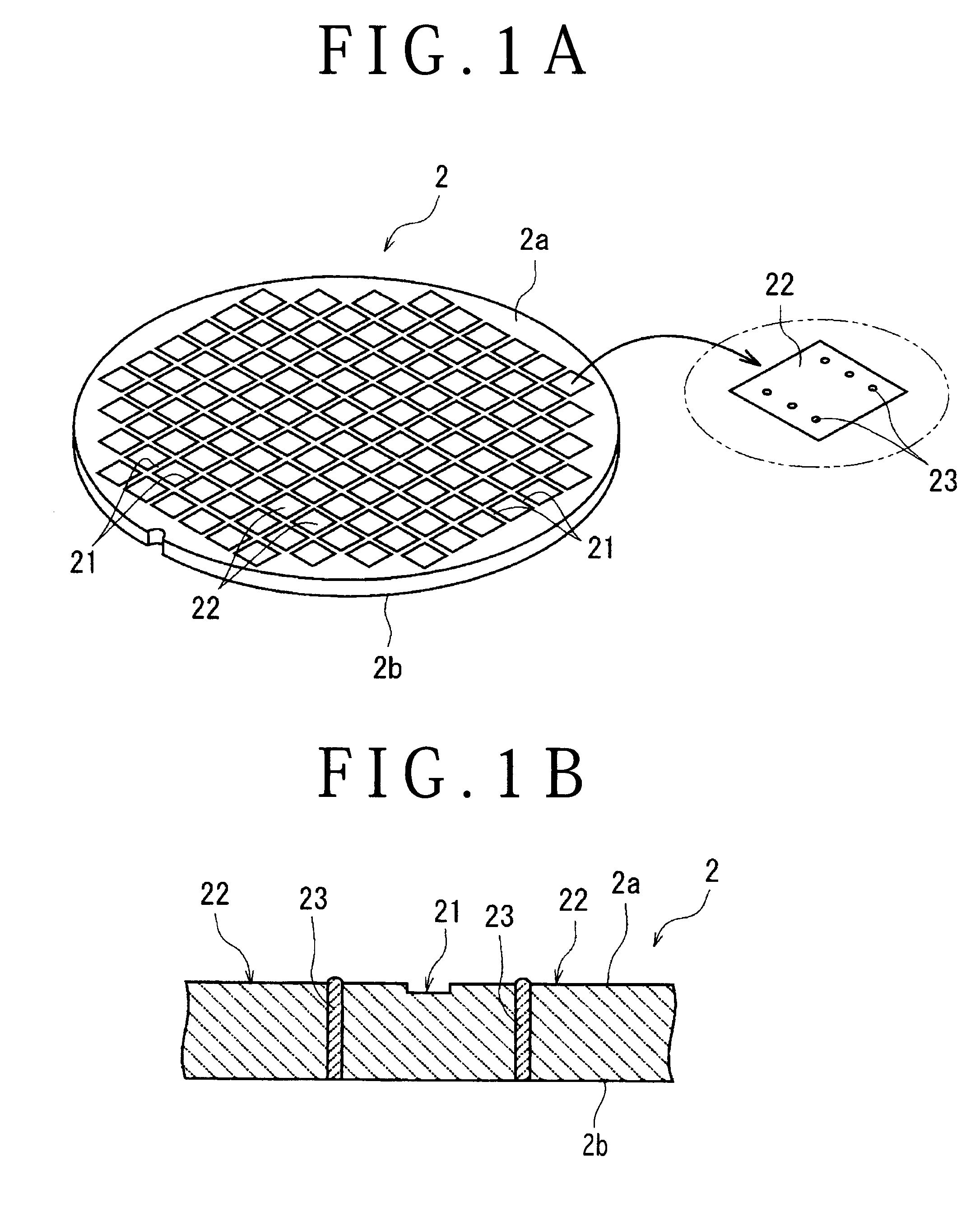
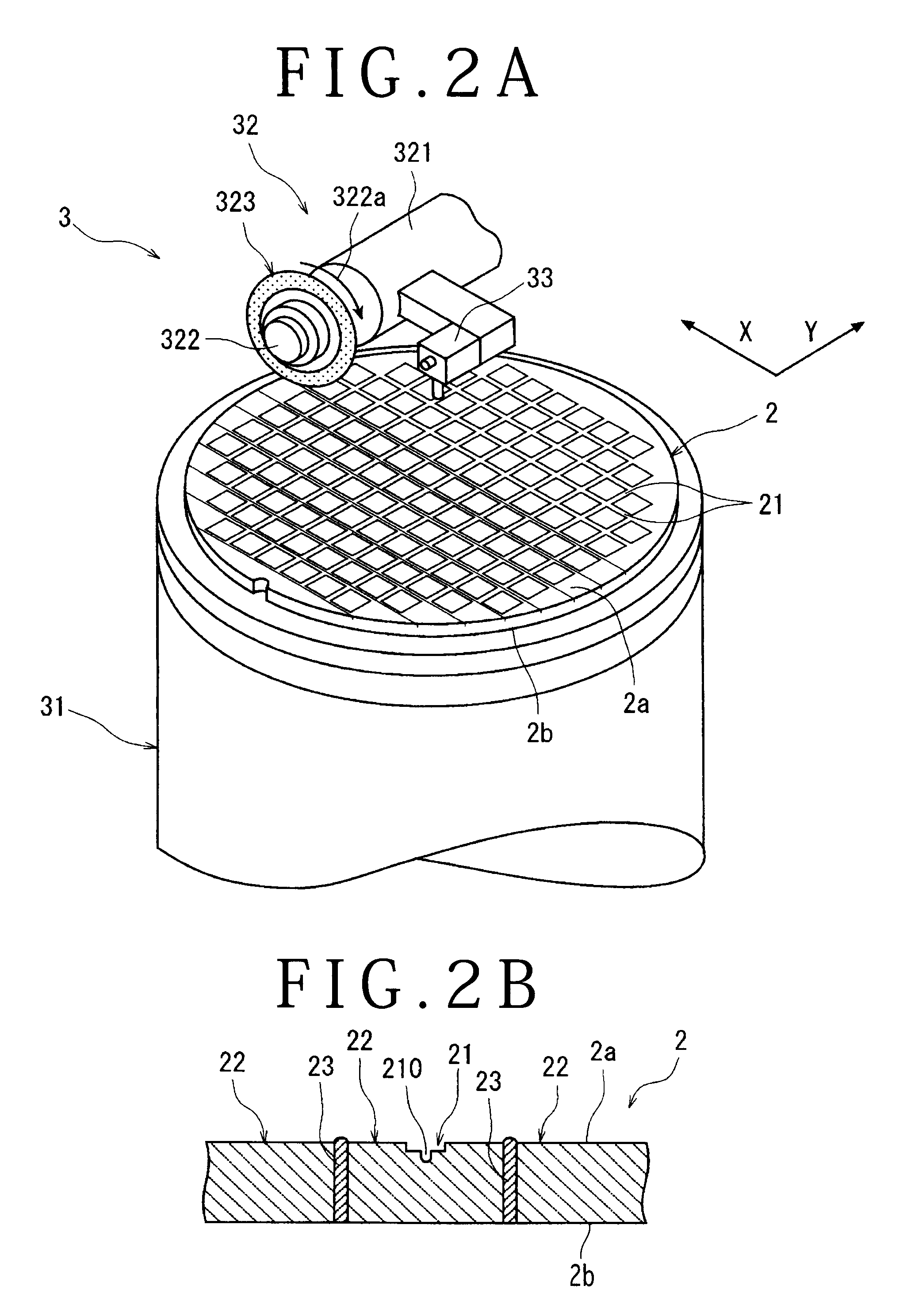
[0069]Some preferred embodiments of the stacked device manufacturing method according to the present invention will now be described in detail with reference to the attached drawings. FIG. 1A is a perspective view of a semiconductor wafer 2 as a wafer. The semiconductor wafer 2 shown in FIG. 1A is a silicon wafer having a thickness of 600 μm, for example. The semiconductor wafer 2 has a front side 2a and a back side 2b. A plurality of crossing streets 21 are formed on the front side 2a of the semiconductor wafer 2 to thereby partition a plurality of rectangular regions where a plurality of devices 22 such as ICs and LSIs are respectively formed. As shown in FIG. 1B, each device 22 of the semiconductor wafer 2 is provided with a plurality of electrodes 23 extending from the front side 2a to the back side 2b.

[0070]A first preferred embodiment of the stacked device manufacturing method according to the present invention will now be described with reference to FIGS. 2A to 14B, wherein ...


PUM


Abstract

A stacked device manufacturing method including a kerf forming step of forming a kerf on the front side of each of plural wafers along each street, the kerf having a depth corresponding to a predetermined finished thickness of each wafer, a first stacking step of stacking a first one of the wafers and a second one of the wafers in such a manner that the front side of the second wafer is opposed to the front side of the first wafer and that the electrodes of the second wafer are respectively bonded to the electrodes of the first wafer, a first back grinding step of grinding the back side of the second wafer to expose each kerf of the second wafer to the back side of the second wafer, a second stacking step of stacking a third one of the wafers to the second wafer in such a manner that the front side of the third wafer is opposed to the back side of the second wafer and that the electrodes of the third wafer are respectively bonded to the electrodes of the second wafer, and a second back grinding step of grinding the back side of the third wafer to expose each kerf of the third wafer to the back side of the third wafer.

Description

BACKGROUND OF THE INVENTION[0001]1. Field of the Invention[0002]The present invention relates to a manufacturing method for a stacked device composed of a plurality of semiconductor chips stacked together, each semiconductor chip being formed with a device such as IC and LSI on the front side.[0003]2. Description of the Related Art[0004]In a semiconductor device fabrication process, a plurality of crossing streets (division lines) are formed on the front side of a substantially disk-shaped semiconductor wafer to partition a plurality of regions where devices such as ICs and LSIs are respectively formed. The semiconductor wafer having the devices in the partitioned regions is divided along the streets to manufacture a plurality of individual semiconductor chips. For the purposes of size reduction and higher functionality of equipment, a stacked device composed of a plurality of semiconductor chips stacked together has been put to practical use. This stacked device is manufactured by ...

Claims


Application Information

Patent Timeline
IPC IPC(8): H01L21/50
CPCH01L21/6836H01L25/0657H01L25/50H01L2221/68327H01L2221/68336H01L2924/0002H01L2225/06513H01L2225/06541H01L2924/00
Inventor NAKAMURA, MASARU
Owner DISCO CORP
Why Eureka
Try Eureka