Gapfill improvement with low etch rate dielectric liners

a dielectric liner and low etching rate technology, applied in the field of manufacturing technology, can solve the problems of increasing undesirable electrical interactions between adjacent circuit elements, reducing the width of these trenches, and increasing the aspect ratio of the trench

Inactive Publication Date: 2010-04-22
APPLIED MATERIALS INC
View PDF25 Cites 313 Cited by
  • Summary
  • Abstract
  • Description
  • Claims
  • Application Information

AI Technical Summary

Benefits of technology

[0009]In yet another embodiment, a method of depositing a film to fill a gap in a surface of a substrate includes forming a dielectric liner on the surface of the substrate, in which a silicon oxide to dielectric liner etch ratio is greater than about 50. The method further includes depositing a first layer of dielectric on the dielectric liner, etching the surface of the substrate and depositing a second layer of dielectric to substantially fill the gap.

Problems solved by technology

The increased density can increase undesirable electrical interactions between adjacent circuit elements and conducting lines.
As circuit densities increase, however, the widths of these trenches decrease, increasing their aspect ratios and making it progressively more difficult to fill the trenches without leaving voids.
A trench which is not completely filled is undesirable since the degree of isolation may be compromised, thus limiting the maximum operational frequency or otherwise adversely affecting operation of the integrated circuit.
The high reactivity of the species in the plasma reduces the energy required for a chemical reaction to take place, and thus lowers the temperature required for such CVD processes when compared with conventional thermal CVD processes.
The etching step can penetrate through deposited material and damage underlying layers especially near the tops of trenches or vias.
In the case of shallow trench isolation (STI) the underlying semiconductor and / or protective silicon nitride barrier layer may be damaged which can cause device instability.
Device reliability is generally at risk when the etching step is allowed to remove too much material.

Method used


Image

  • Gapfill improvement with low etch rate dielectric liners
  • Gapfill improvement with low etch rate dielectric liners
  • Gapfill improvement with low etch rate dielectric liners

Examples


Embodiment Construction

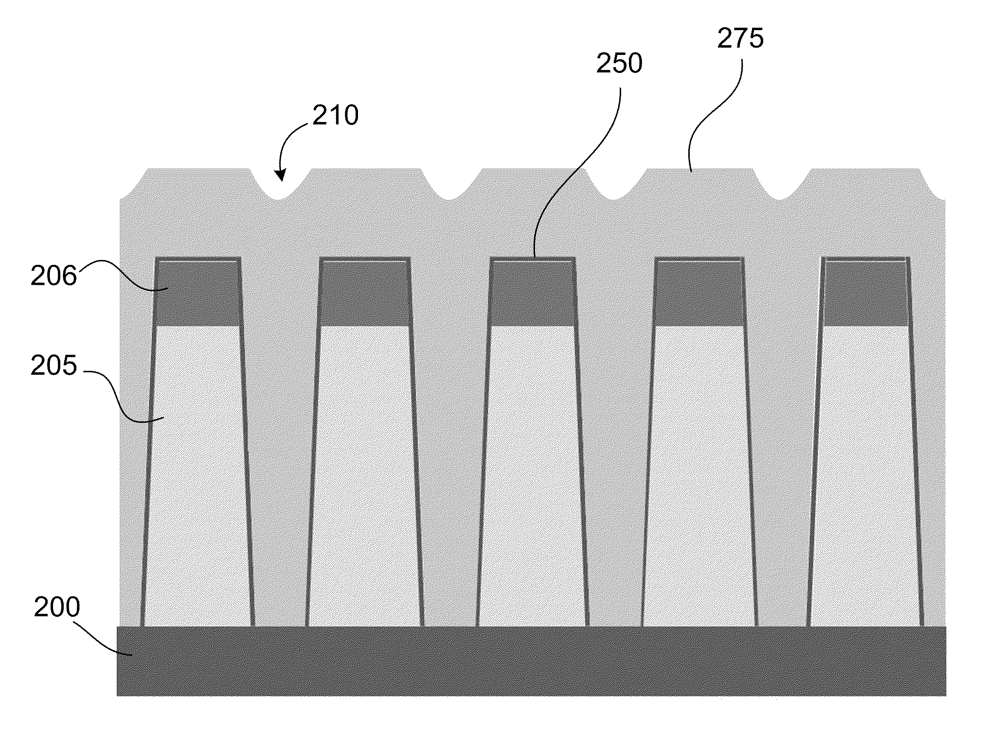
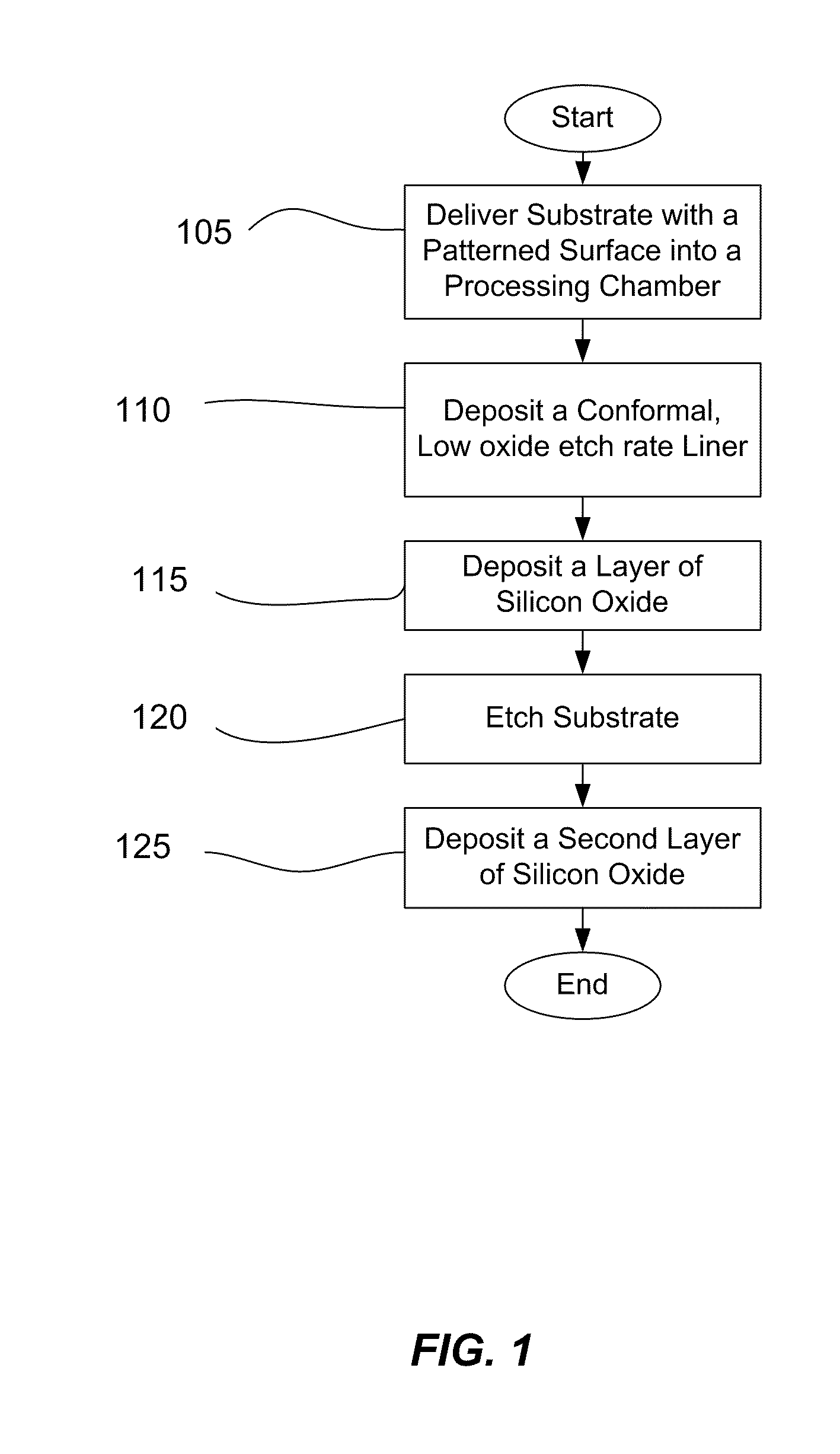
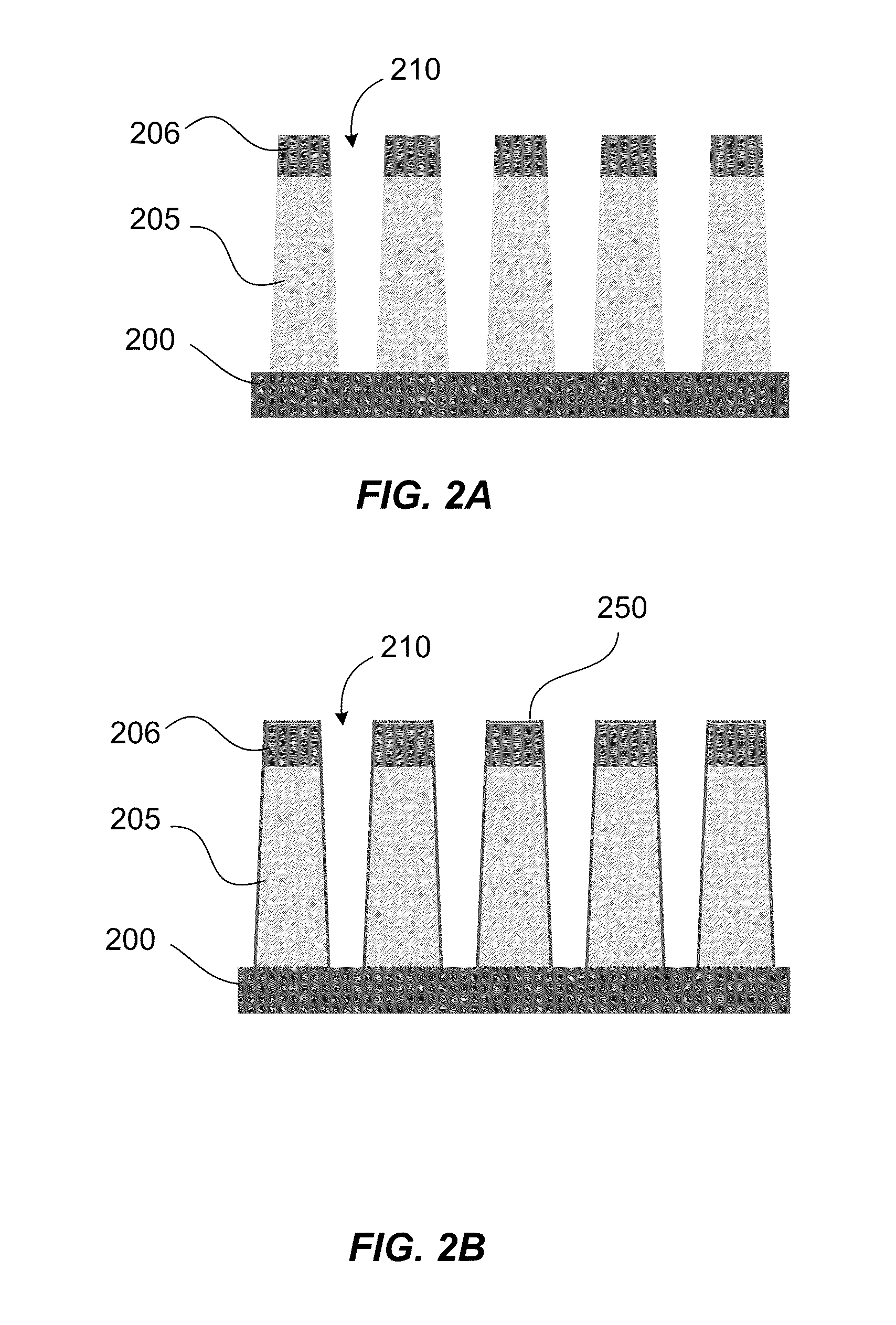
[0017]A method of filling a trench is described and includes depositing a dielectric liner with a high ratio of silicon oxide to dielectric liner etch rate in fluorine-containing etch chemistries. Silicon oxide is deposited within the trench and etched to reopen or widen a gap near the top of the trench. The dielectric liner protects the underlying substrate during the etch process so the gap can be made wider. Silicon oxide is deposited within the trench again to fill the trench.

[0018]Embodiments of the invention are directed to methods of depositing a film to fill a trench in a surface of a substrate. For trenches of a given width, embodiments use a multistep deposition and etching process in which the etching process occurs between deposition processes to widen or reopen a gap within the film. A dielectric liner layer having a low HF etch rate relative to silicon oxide is deposited conformally on a trench in the surface of the substrate and followed by a silicon oxide dep / etch / de...


PUM


Abstract

A method of filling a trench is described and includes depositing a dielectric liner with a high ratio of silicon oxide to dielectric liner etch rate in fluorine-containing etch chemistries. Silicon oxide is deposited within the trench and etched to reopen or widen a gap near the top of the trench. The dielectric liner protects the underlying substrate during the etch process so the gap can be made wider. Silicon oxide is deposited within the trench again to substantially fill the trench.

Description

CROSS-REFERENCES TO RELATED APPLICATIONS[0001]This application claims the benefit of U.S. Provisional Application No. 61 / 106,076 by Kwon et al, filed Oct. 16, 2008 and titled “GAPFILL IMPROVEMENT WITH HIGH LOW ETCH RATE DIELECTRIC LINERS”. This application is related to U.S. patent application Ser. No. 11 / 765,257 and U.S. Pat. Prov. App. Ser. No. 61 / 042,638, both titled “BORON NITRIDE AND BORON NITRIDE-DERIVED MATERIALS DEPOSITION METHOD.” The entire contents of all three applications are herein incorporated by reference for all purposes.FIELD[0002]This application relates to manufacturing technology solutions involving equipment, processes, and materials used in the deposition, patterning, and treatment of thin-films and coatings, with representative examples including (but not limited to) applications involving: semiconductor and dielectric materials and devices, silicon-based wafers and flat panel displays (such as TFTs).BACKGROUND[0003]Increasing the density of integrated circui...

Claims


Application Information

Patent Timeline
Patent Type & Authority Applications(United States)
IPC IPC(8): H01L21/762H01L21/31
CPCH01L21/02112H01L21/02247H01L21/76224H01L21/318H01L21/02304H01L21/762
Inventor KWON, YOUNG SOOJANG, BIWANG, ANCHUANLEE, YOUNG S.BALSEANU, MIHAELAXIA, LI-QUNJEON, JIN HO
Owner APPLIED MATERIALS INC
Why Eureka
Try Eureka