Printed circuit board

a printed circuit board and circuit board technology, applied in printed circuit aspects, cross-talk/noise/interference reduction, metallic pattern materials, etc., can solve problems such as increasing the size of the ground layer, increasing the size of the pcb, and emi problems

Inactive Publication Date: 2010-04-29
HONG FU JIN PRECISION IND (SHENZHEN) CO LTD +1
View PDF6 Cites 8 Cited by
  • Summary
  • Abstract
  • Description
  • Claims
  • Application Information

AI Technical Summary

Problems solved by technology

At the edges of the power layer and the ground layer, electromagnetic field lines fringe outward from the PCB, causing external electromagnetic interference (EMI) problems.
However, increasing the size of the ground layer substantially increases the size of the PCB.
This is not beneficial for miniaturization of the PCB.
Moreover, decreasing the size of the power layer limits the space for circuit design.

Method used


Image

  • Printed circuit board
  • Printed circuit board
  • Printed circuit board

Examples


Embodiment Construction

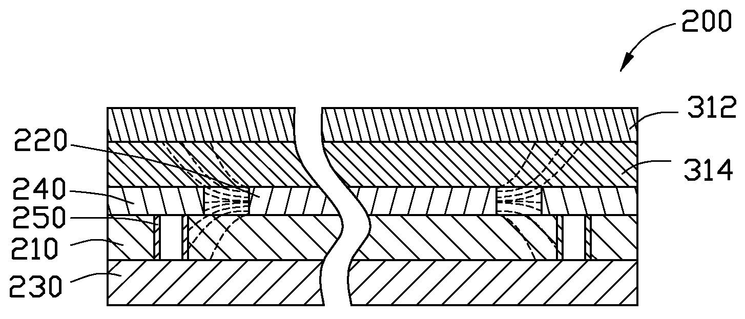
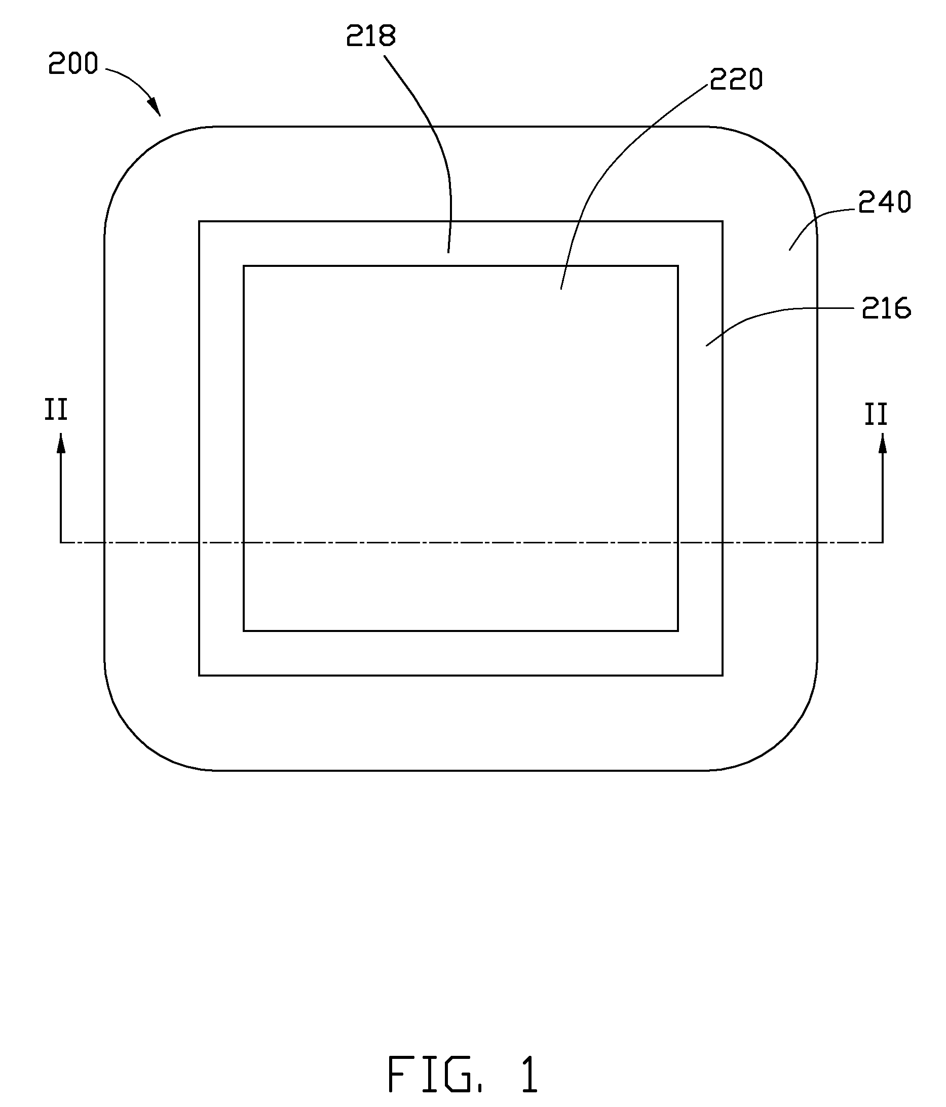
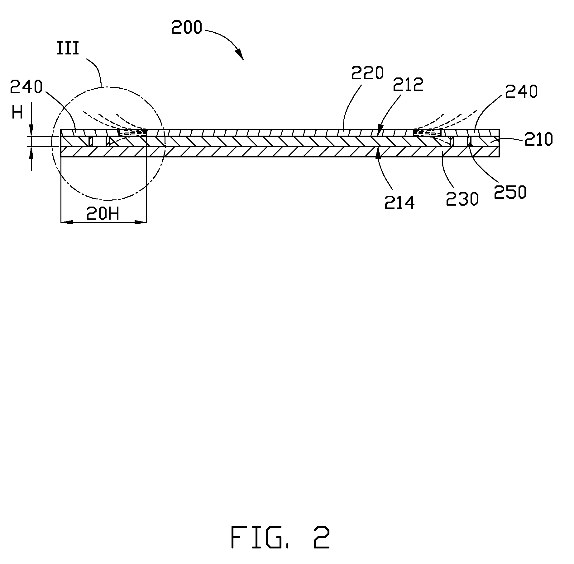
[0010]Referring to FIGS. 1-2, a PCB 200, according to an exemplary embodiment of the present disclosure, includes a dielectric layer 210, a power layer 220, a ground layer 230, and an EMI reducing layer 240.

[0011]The dielectric layer 210 is made of a dielectric material such as bakelite resin, fiberglass, epoxy resin, or glass-epoxy resin. In this embodiment, the dielectric layer 210 is made of glass-epoxy resin. The dielectric layer 210 includes a first surface 212 and a second surface 214. The dielectric layer 210 defines a number of via holes 250 through a periphery portion 216 of the dielectric layer 210 (i.e., through the first surface 212 and the second surface 214).

[0012]The power layer 220 is configured for electrically powering the PCB 200. The ground layer 230 is configured for electrically grounding the PCB 200. The EMI reducing layer 240 is configured for reducing EMI generated by the PCB 200 radiating outwardly (see below). The power layer 220, the ground layer 230, the...


PUM


Abstract

A printed circuit board (PCB) is disclosed. The PCB includes a dielectric layer, a power layer, a ground layer, and an electromagnetic interference reducing layer. The dielectric layer includes a central portion and a periphery portion surrounding the central portion. The dielectric layer defines a number of via holes through the periphery portion. The ground layer is adhered to a surface of the dielectric layer, covering both the central portion and the periphery portion. The power layer and the EMI reducing layer are separately adhered to another surface of the dielectric layer facing away from the conductive ground layer. The conductive power layer covers the central portion. The EMI reducing layer substantially covers the periphery portion and is electrically connected to the ground layer via the via holes.

Description

BACKGROUND[0001]1. Technical Field[0002]The present disclosure relates to printed circuit boards (PCBs) and, particularly, to a PCB capable of reducing external electromagnetic interference (EMI).[0003]2. Description of Related Art[0004]A PCB typically includes a power layer for powering the PCB and a ground layer for grounding the PCB. At the edges of the power layer and the ground layer, electromagnetic field lines fringe outward from the PCB, causing external electromagnetic interference (EMI) problems. To reduce EMI, it is proposed that the ground layer must be sized larger than the power layer. It also has been experientially proved that the larger a size difference between the ground layer and the power layer is, the more excellent EMI reduction can be achieved. The size difference between the ground layer and the power layer can be increased in two ways: increasing the size of the ground layer and decreasing the size of the power layer. However, increasing the size of the gro...

Claims


Application Information

Patent Timeline
Patent Type & Authority Applications(United States)
IPC IPC(8): H05K1/09H05K1/00
CPCH05K1/0218H05K2201/0715H05K2201/09618H05K2201/09345H05K2201/09354H05K2201/09309
Inventor FAN, FA-PING
Owner HONG FU JIN PRECISION IND (SHENZHEN) CO LTD
Why Eureka
Try Eureka