Acoustic assisted single wafer wet clean for semiconductor wafer process

a technology of semiconductor wafers and wafers, applied in the direction of cleaning processes and apparatus, cleaning using liquids, cleaning processes using liquids, etc., can solve the problems of reducing the reliability and yield of the resulting device from the fabrication operation using ultrasonic cleaning, affecting the features around which the submicron particle contaminants are deposited, and affecting the cleaning effect of the substrate surface. , to achieve the effect of improving the cleaning chemistries

Inactive Publication Date: 2010-05-06
LAM RES CORP
View PDF12 Cites 23 Cited by
  • Summary
  • Abstract
  • Description
  • Claims
  • Application Information

AI Technical Summary

Benefits of technology

[0011]Broadly speaking, the present invention fills these needs by providing a cleaning tool that is capable of managing, in a controlled and effective manner, the application of acoustic energy and enhanced cleaning chemistries t...

Problems solved by technology

Due to the critical dimensions of the submicron particles, cleaning techniques using low-frequency ultrasonic energy are no longer capable of effectively removing the submicron particles from around the features.
As a result, the reliability and yield of the resulting devices from the fabrication operation using ultrasonic cleaning are substantially reduced.
Although the acoustic energy used in the megas...

Method used


Image

  • Acoustic assisted single wafer wet clean for semiconductor wafer process
  • Acoustic assisted single wafer wet clean for semiconductor wafer process
  • Acoustic assisted single wafer wet clean for semiconductor wafer process

Examples


Embodiment Construction

[0035]An invention for methods and apparatuses for cleaning and / or drying a substrate is disclosed. In the following description, numerous specific details are set forth in order to provide a thorough understanding of the present invention. It will be understood, however, by one of ordinary skill in the art, that the present invention may be practiced without some or all of these specific details. In other instances, well known process operations have not been described in detail in order not to unnecessarily obscure the present invention.

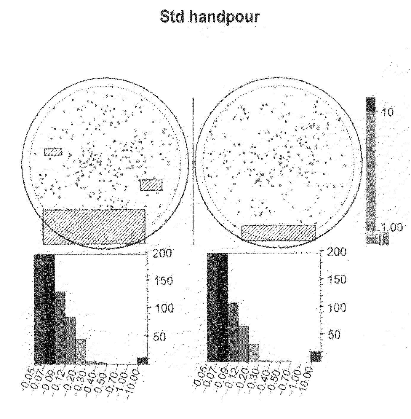
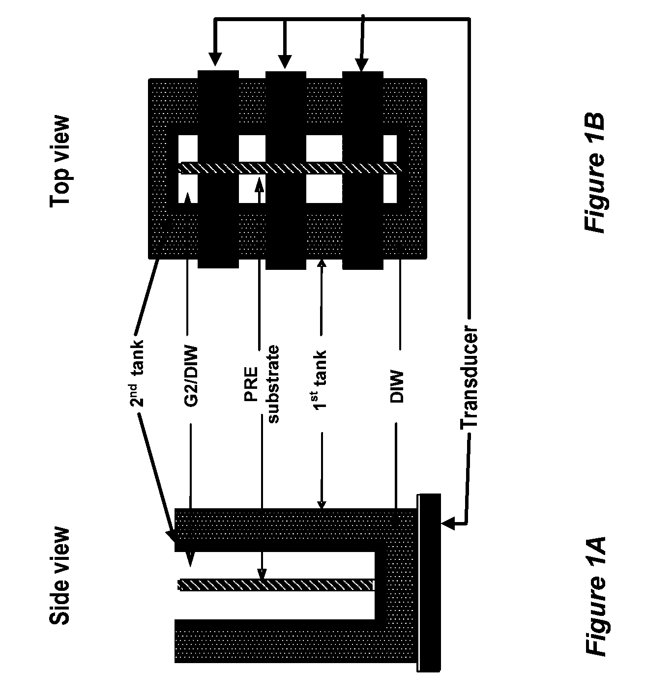
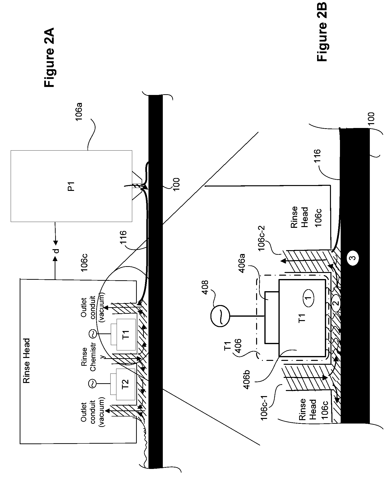
[0036]FIGS. 1A and 1B illustrate an embodiment of a substrate processing system. In this embodiment, a dip tank is used for processing a substrate. It should be appreciated that the substrate processing system illustrated in FIGS. 1A and 1B is exemplary, and that any other suitable type of configuration that would enable cleaning a substrate surface using a dip tank may be utilized. FIGS. 1A and 1B illustrate a side and a top view of a dip tank sys...


PUM

PropertyMeasurementUnit
Frequencyaaaaaaaaaa
Temperatureaaaaaaaaaa
Thicknessaaaaaaaaaa

Abstract

A method for cleaning a substrate is provided that includes applying a liquid medium to a surface of the substrate such that the liquid medium substantially covers a portion of the substrate that is being cleaned. One or more transducers are used to generate acoustic energy. The generated acoustic energy is applied to the substrate and the liquid medium meniscus such that the applied acoustic energy to the liquid medium prevents cavitation within the liquid medium. The acoustic energy applied to the substrate provides maximum acoustic wave displacement to acoustic waves introduced into the liquid medium. The acoustic energy introduced into the substrate and the liquid medium enables dislodging of the particle contaminant from the surface of the substrate. The dislodged particle contaminants become entrapped within the liquid medium and are carried away from the surface of the substrate by the liquid medium.

Description

CROSS REFERENCE TO RELATED APPLICATION[0001]This application is related to U.S. patent application Ser. No. 12 / 131654 (Attorney Docket No. LAM2P628A) filed on Jun. 2, 2008, and entitled “MATERIALS FOR PARTICLE REMOVAL BY SINGLE-PHASE AND TWO-PHASE MEDIA.” This application is also related to U.S. patent application Ser. No. 12 / 165,577 (Attorney Docket No. LAM2P638), filed on Jun. 30, 2008, entitled “SINGLE SUBSTRATE PROCESSING HEAD FOR PARTICLE REMOVAL USING LOW VISCOSITY FLUID.” The aforementioned patent applications are incorporated herein by reference.BACKGROUND OF THE INVENTION[0002]1. Field of the Invention[0003]The present invention relates generally to the cleaning of a semiconductor substrate and, more particularly, to a method and apparatus for utilizing acoustic energy in combination with selective cleaning media to clean a semiconductor substrate following fabrication processes.[0004]2. Description of the Related Art[0005]In the semiconductor chip fabrication process, it i...

Claims


Application Information

Patent Timeline
IPC IPC(8): B08B3/12
CPCH01L21/67051H01L21/302
Inventor PENG, GRANTMUI, DAVIDKON, SHIH-CHUNG
Owner LAM RES CORP
Why Eureka
Try Eureka