Semiconductor memory device and manufacturing method for semiconductor memory device

a semiconductor memory and memory device technology, applied in semiconductor devices, digital storage, instruments, etc., can solve the problems of increasing the risk of malfunction, and increasing the magnetic interference between memory cells

Active Publication Date: 2010-05-06
KIOXIA CORP
View PDF5 Cites 30 Cited by
  • Summary
  • Abstract
  • Description
  • Claims
  • Application Information

AI Technical Summary

Problems solved by technology

However, in the method disclosed in Japanese Patent Application Laid-open No. 2003-218328, because both sides of an impurity deposition are coated with a gate deposition, a shielding effectiveness of flux generated by a current that passes through the impurity deposition is not sufficiently high

Method used


Image

  • Semiconductor memory device and manufacturing method for semiconductor memory device
  • Semiconductor memory device and manufacturing method for semiconductor memory device
  • Semiconductor memory device and manufacturing method for semiconductor memory device

Examples


first embodiment

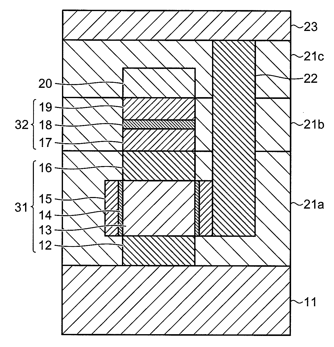
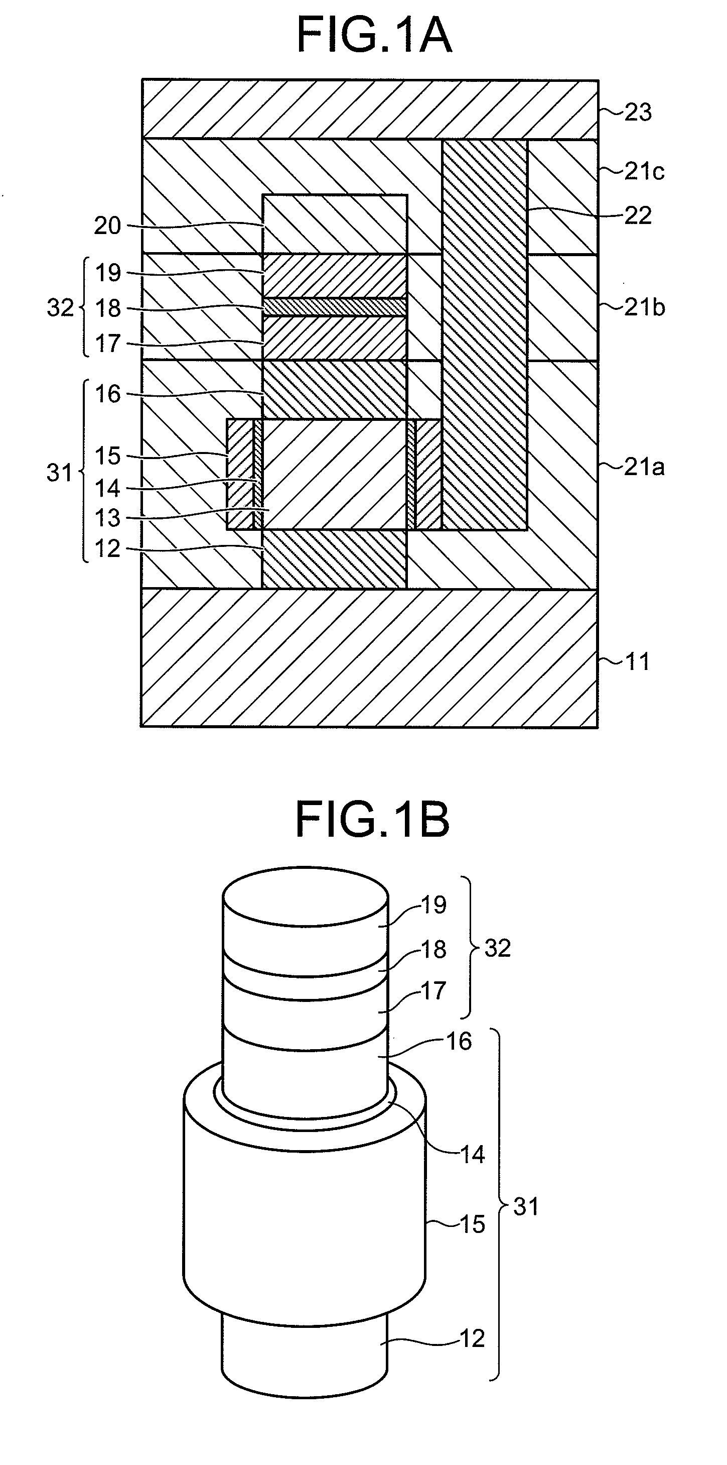
[0053]In the first embodiment, the configuration including the magnetic layer 17, the nonmagnetic layer 18, and the magnetic layer 19 has been explained as the spin-injection magnetization-reversal element 32. The spin-injection magnetization-reversal element 32 can have other configurations. For example, upper and lower electrodes can be placed on and underneath the spin-injection magnetization-reversal element 32. An antiferromagnetic layer can be provided to fix magnetization of the magnetic fixed layer. A double pin configuration can be used as well as a single pin configuration.

[0054]Configurations of the spin-injection magnetization-reversal element 32 other than that shown in FIG. 1A are explained in second and third embodiments of the present invention.

second embodiment

[0055]FIGS. 5A and 5B are cross-sectional views of a schematic configuration of a spin-injection magnetization-reversal element according to the

[0056]In FIGS. 5A and 5B, a spin filter layer 42, a magnetization free layer 43, a nonmagnetic layer 44, a magnetization fixed layer 45, and an antiferromagnetic layer 46 are successively deposited on a magnetization fixed layer 41. For example, it is possible to use CoFe as materials for the magnetization fixed layers 41 and 45 and the magnetization free layer 43, Ru as a material for the spin filter layer 42, Cu as a material for the nonmagnetic layer 44, and IrMn as a material for the antiferromagnetic layer 46.

[0057]When a current I− vertically flows through the magnetization fixed layer 41, the spin filter layer 42, the magnetization free layer 43, the nonmagnetic layer 44, the magnetization fixed layer 45, and the antiferromagnetic layer 46, electrons e having up spin are injected from the magnetization fixed layer 45 to the magnetizat...

third embodiment

[0060]FIG. 6 is a cross-sectional view of a schematic configuration of a spin-injection magnetization-reversal element according to the

[0061]In FIG. 6, a vertical-magnetization pinning layer 52, an interface magnetic layer 53, a tunnel film 54, an interface magnetic layer 55, and a vertical-magnetization free layer 56 are successively deposited on an electrode 51. It is possible to use CoFeB as materials for the interface magnetic layers 53 and 55, and MgO as a material for the tunnel film 54, for example.

[0062]When a vertical magnetic film is used for the magnetization fixed layer and the magnetization free layer in the spin-injection magnetization-reversal element, the spin-injection magnetization-reversal element can be brought less subject to a diamagnetic field as compared to an in-plane magnetization method. Accordingly, an energy level during the magnetization reversal can be lowered and a write current can be reduced.

[0063]FIG. 7 is a cross-sectional view of a schematic conf...


PUM


Abstract

A channel layer is deposited on a first impurity layer, a second impurity layer is deposited on the channel layer, a gate electrode is placed to surround a circumference of the channel layer with a gate insulating film interposed therebetween, a spin-injection magnetization-reversal element is deposited on the second impurity layer, a bit line is placed on the spin-injection magnetization-reversal element, and a word line is placed on the bit line to be electrically connected to the gate electrode.

Description

CROSS-REFERENCE TO RELATED APPLICATIONS[0001]This application is based upon and claims the benefit of priority from the prior Japanese Patent Application No. 2008-283276, filed on Nov. 4, 2008; the entire contents of which are incorporated herein by reference.BACKGROUND OF THE INVENTION[0002]1. Field of the Invention[0003]The present invention relates to a semiconductor memory device and a manufacturing method for a semiconductor memory device, and, more particularly to a semiconductor memory device and a manufacturing method for a semiconductor memory device preferably applied to a magnetic random access memory (MRAM) in which a magnetoresistive element that magnetically stores information therein is deposited on a selection transistor.[0004]2. Description of the Related Art[0005]The MRAM is attracting attention as a semiconductor memory device having high-speed accessibility similar to that of a static RAM (SRAM), a high degree of integration similar to that of a dynamic RAM (DRAM...

Claims


Application Information

Patent Timeline
IPC IPC(8): H01L43/06H01L43/12
CPCH01L27/228G11C11/161G11C11/1659H10B61/22
Inventor KUSHIDA, KEIICHI
Owner KIOXIA CORP
Why Eureka
Try Eureka