Solid-state imaging device, method for manufacturing the same, and electronic apparatus

a solid-state imaging and manufacturing method technology, applied in the direction of radioation control devices, television systems, television system scanning details, etc., can solve the problems of loss due to electrostatic shielding of visible light, large wavelength of visible light, and disadvantageous decrease in sensitivity beyond the area ratio between the opening of the pixel and the interpixel light-shielding film, etc., to achieve increased suppress false signals, and increase sensitivity in small pixels

Inactive Publication Date: 2010-05-06
SONY CORP
View PDF6 Cites 97 Cited by
  • Summary
  • Abstract
  • Description
  • Claims
  • Application Information

AI Technical Summary

Benefits of technology

[0030]With this configuration including the solid-state imaging device having the nonconductive interpixel light-shielding film, reflection of light does not occur in the interpixel light-shielding film, so that reflection between an imaging lens and the solid-state imaging device can be prevented.
[0031]According to the above-described solid-state imaging device, the sensitivity in small pixels can be increased. Also, false signals can be suppressed.
[0032]According to the above-described method, a solid-state imaging device with an increased sensitivity in small pixels and suppressed false signals can be manufactured.
[0033]According to the above-described electronic apparatus, the sensitivity can be increased and false signals can be suppressed even when pixels of a reduced size are used in the solid-state imaging device. Accordingly, a miniaturized high-quality electronic apparatus can be provided.

Problems solved by technology

In the CMOS solid-state imaging device including the light-shielding metal 141 that shields areas between pixels illustrated in FIG. 8, the sensitivity disadvantageously decreases beyond an area ratio between openings of pixels and an interpixel light-shielding film as the pixels become smaller.
Particularly, if an opening width of the pixels is 3 μm or less in smaller pixels, the wavelength of visible light is considerable, and losses due to electrostatic shielding of visible light occur.
If the opening width of pixels is 3 μm or less, the wavelength of visible light is considerable and a diffraction effect of visible light is also considerable, so that a light focusing effect of on-chip lenses is inadequate.

Method used


Image

  • Solid-state imaging device, method for manufacturing the same, and electronic apparatus
  • Solid-state imaging device, method for manufacturing the same, and electronic apparatus
  • Solid-state imaging device, method for manufacturing the same, and electronic apparatus

Examples


first embodiment

Exemplary Configuration of Solid-State Imaging Device

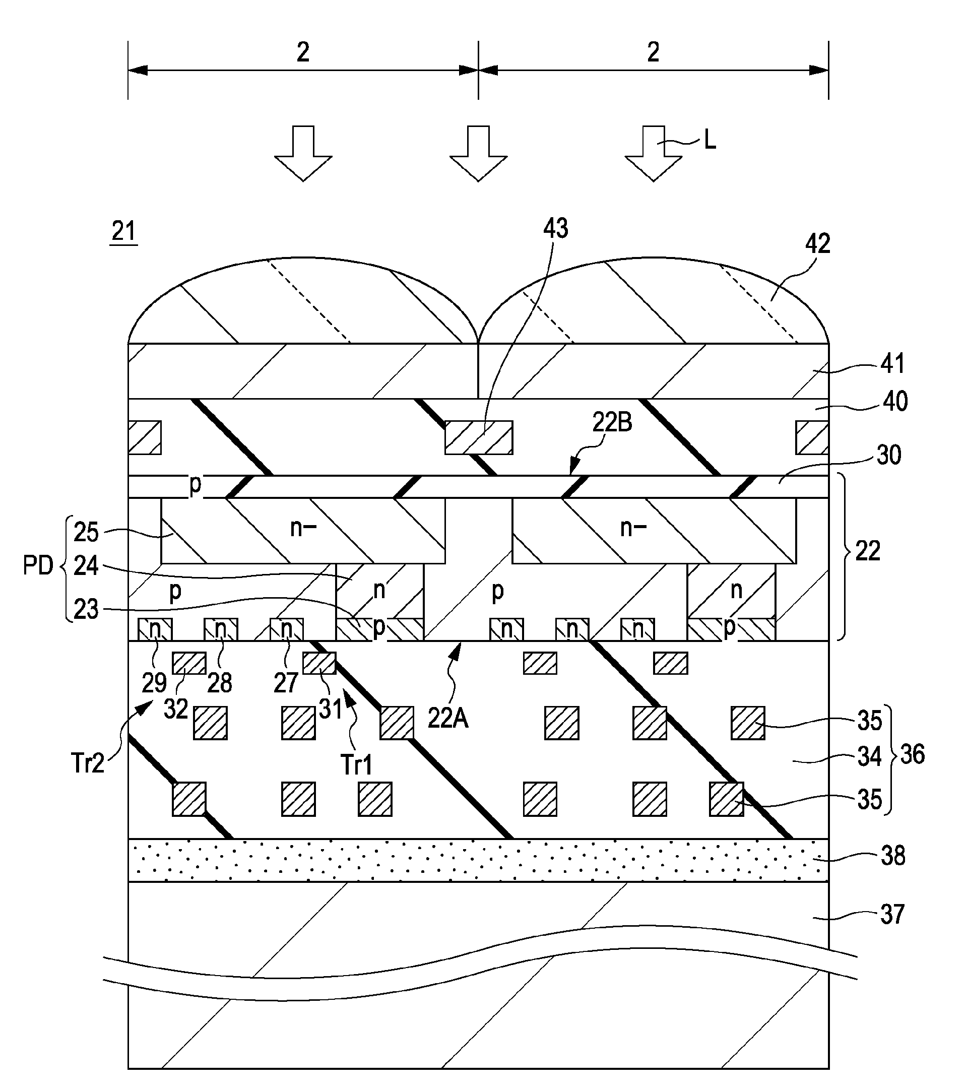
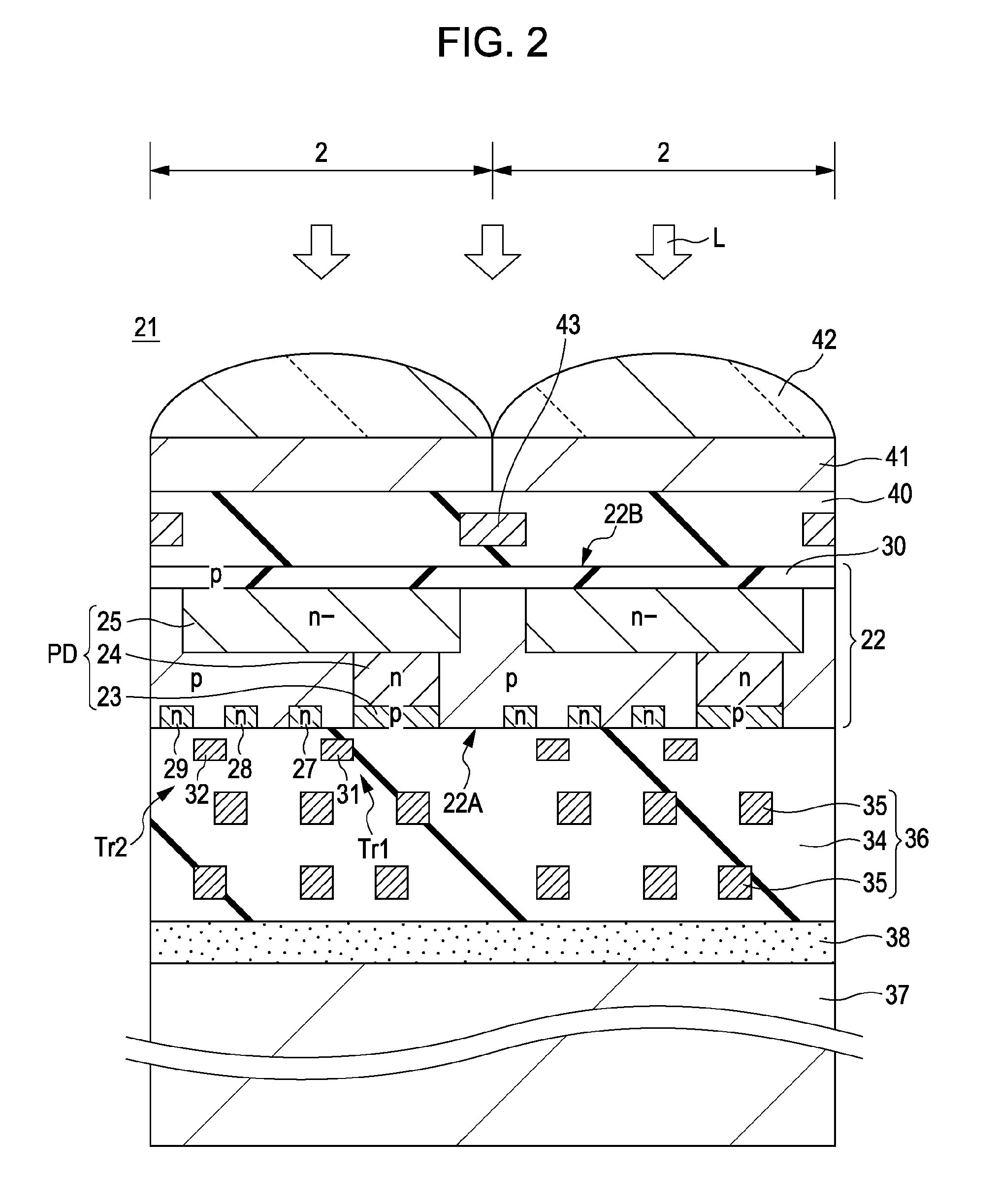
[0052]FIG. 2 illustrates a solid-state imaging device 21 according to a first embodiment of the present invention. The solid-state imaging device 21 according to this embodiment is applied to a back-illuminated CMOS solid-state imaging device. FIG. 2 illustrates a main part of the effective pixel portion 3A of the pixel unit 3 illustrated in FIG. 1. In FIG. 2, a surface irradiated with incident light L of a silicon portion 22 is a back surface 22B, and the opposite surface is a front surface 22A.

[0053]In the solid-state imaging device 21 according to the first embodiment, a plurality of pixels including photodiodes PD serving as photoelectric conversion elements and a plurality of pixel transistors are arrayed and formed in a two-dimensional matrix pattern in a silicon portion (corresponding to a semiconductor substrate) 22. The silicon portion 22 is a first conductivity type (p-type in this embodiment) silicon portion. On the fro...

second embodiment

Exemplary Configuration of Solid-State Imaging Device

[0081]FIG. 6 illustrates a solid-state imaging device 51 according to a second embodiment of the present invention.

[0082]The solid-state imaging device 51 according to this embodiment is applied to the back-illuminated CMOS solid-state imaging device. FIG. 6 illustrates a main part of the effective pixel portion 3A of the pixel unit 3. In FIG. 6, as in FIG. 1, a surface irradiated with incident light L of the silicon portion 22 is the back surface 22B, and the opposite surface is the front surface 22A.

[0083]In the solid-state imaging device 51 according to the second embodiment, the interlayer insulating film 40 is formed on the back surface 22B of the silicon portion 22, the nonconductive interpixel light-shielding film 43 is formed on the interlayer insulating film 40, and the on-chip color filters 41 are directly formed on the interpixel light-shielding film 43 that is not planarized. The on-chip lenses 42 are formed on the on-...

third embodiment

Exemplary Configuration of Solid-State Imaging Device

[0088]A solid-state imaging device according to an embodiment of the present invention can be applied to a CCD solid-state imaging device. Although not illustrated, the CCD solid-state imaging device includes a plurality of light receiving units, a CCD-structure vertical transfer register corresponding to columns of the respective light receiving units, a CCD-structure horizontal transfer register, and an output unit. The light receiving units include photodiodes serving as photoelectric conversion elements formed on a semiconductor substrate. The vertical and horizontal transfer registers are formed by arraying a plurality of transfer electrodes in a charge transfer direction in an on-channel region via a gate insulating film. Each light receiving unit and the transfer electrode corresponding to the light receiving unit in the vertical transfer register constitute a unit pixel.

[0089]A pixel unit includes an effective pixel portio...


PUM


Abstract

A solid-state imaging device includes an effective pixel portion in which a plurality of pixels including photoelectric conversion elements are arrayed; and a nonconductive interpixel light-shielding film that is placed in the effective pixel portion and that shields areas between the pixels.

Description

BACKGROUND OF THE INVENTION[0001]1. Field of the Invention[0002]The present invention relates to a solid-state imaging device, a method for manufacturing the same, and an electronic apparatus.[0003]2. Description of the Related Art[0004]Solid-state imaging devices are broadly classified into amplified solid-state imaging devices represented by CMOS (Complementary Metal Oxide Semiconductor) image sensors and charge-transfer solid-state imaging devices represented by CCD (Charge Coupled Device) image sensors. These types of solid-state imaging devices are widely used in digital still cameras and digital video cameras. In recent years, the CMOS image sensors have often been used as solid-state imaging devices mounted on mobile apparatuses, such as camera-equipped mobile phones or PDAs (Personal Digital Assistants), from the viewpoint of low power supply voltages and power consumption.[0005]So-called back-illuminated CMOS image sensors, in which light enters from a back side of a substr...

Claims


Application Information

Patent Timeline
Patent Type & Authority Applications(United States)
IPC IPC(8): H04N5/225H01L31/0232H01L21/00H01L27/14H04N5/335H04N5/357H04N5/369H04N5/374
CPCH01L27/14621H01L27/14623H01L27/14627H01L27/14643H01L27/1464H01L27/146
Inventor YANAGITA, TAKESHIMABUCHI, KEIJIINOUE, SUSUMU
Owner SONY CORP
Why Eureka
Try Eureka