Method and System For Coupling Optical Signals Into Silicon Optoelectronic Chips

a technology of optoelectronic chips and optical signals, applied in the field of signal processing, can solve the problems of cable bulk penalties, large power requirements, and complex structure, and achieve only modest improvements in reach and limited scalability

Active Publication Date: 2010-05-06
CISCO TECH INC
View PDF2 Cites 56 Cited by
  • Summary
  • Abstract
  • Description
  • Claims
  • Application Information

AI Technical Summary

Problems solved by technology

They can be mitigated to some extent with equalization, coding, and shielding, but these techniques require considerable power, complexity, and cable bulk penalties while offering only modest improvements in reach and very limited scalability.

Method used


Image

  • Method and System For Coupling Optical Signals Into Silicon Optoelectronic Chips
  • Method and System For Coupling Optical Signals Into Silicon Optoelectronic Chips
  • Method and System For Coupling Optical Signals Into Silicon Optoelectronic Chips

Examples


Embodiment Construction

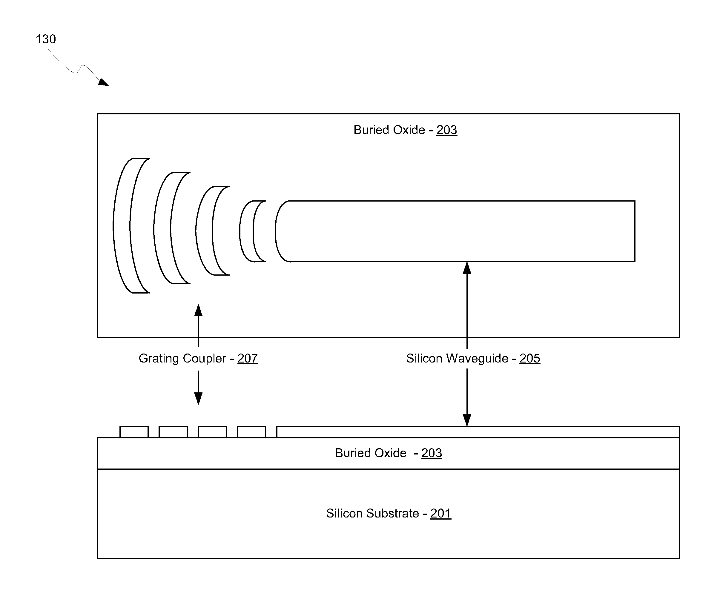
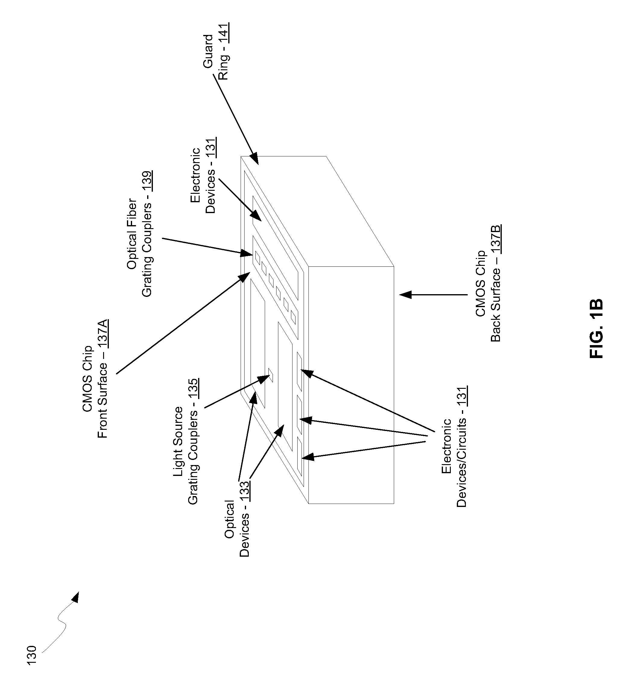
[0017]Certain aspects of the invention may be found in a method and system for coupling optical signals into silicon optoelectronic chips. Exemplary aspects of the invention may comprise coupling one or more optical signals into a back surface of a CMOS photonic chip comprising photonic, electronic, and optoelectronic devices. The photonic, electronic, and optoelectronic devices may be integrated in a front surface of the CMOS photonic chip, and one or more grating couplers may receive the one or more optical signals in the front surface of the CMOS photonic chip. The one or more optical signals may be coupled into the back surface of the CMOS photonic chip via one or more optical fibers, which may be affixed to the CMOS photonic chip utilizing epoxy. The one or more optical signals may be coupled into the back surface of the CMOS photonic chip via one or more optical source assemblies, which may be affixed to the CMOS photonic chip via epoxy. The optical signals may be coupled to t...


PUM


Abstract

A method and system for coupling optical signals into silicon optoelectronic chips are disclosed and may include coupling one or more optical signals into a back surface of a CMOS photonic chip comprising photonic, electronic, and optoelectronic devices. The devices may be integrated in a front surface of the chip and one or more grating couplers may receive the optical signals in the front surface of the chip. The optical signals may be coupled into the back surface of the chip via one or more optical fibers and / or optical source assemblies. The optical signals may be coupled to the grating couplers via a light path etched in the chip, which may be refilled with silicon dioxide. The chip may be flip-chip bonded to a packaging substrate. Optical signals may be reflected back to the grating couplers via metal reflectors, which may be integrated in dielectric layers on the chip.

Description

CROSS-REFERENCE TO RELATED APPLICATIONS / INCORPORATION BY REFERENCE[0001]This application makes reference to and claims priority to U.S. Provisional Application Ser. No. 61 / 198,660 filed on Nov. 6, 2008, which is hereby incorporated herein by reference in its entirety.FEDERALLY SPONSORED RESEARCH OR DEVELOPMENT[0002][Not Applicable]MICROFICHE / COPYRIGHT REFERENCE[0003][Not Applicable]FIELD OF THE INVENTION[0004]Certain embodiments of the invention relate to signal processing. More specifically, certain embodiments of the invention relate to a method and system for coupling optical signals into silicon optoelectronic chips.BACKGROUND OF THE INVENTION[0005]As data networks scale to meet ever-increasing bandwidth requirements, the shortcomings of copper data channels are becoming apparent. Signal attenuation and crosstalk due to radiated electromagnetic energy are the main impediments encountered by designers of such systems. They can be mitigated to some extent with equalization, coding...

Claims


Application Information

Patent Timeline
Patent Type & Authority Applications(United States)
IPC IPC(8): G02B6/34H01L21/50
CPCG02B6/124G02B6/30G02B6/34G02B6/12004G02B2006/12157G02B2006/12104G01J1/0425G02B6/4208G02B2006/12038G02B2006/12061G01J1/02
Inventor PINGUET, THIERRYMEKIS, ATTILAGLOECKNER, STEFFEN
Owner CISCO TECH INC
Why Eureka
Try Eureka