Semiconductor integrated circuit with data bus inversion function

a technology of integrated circuits and data buses, which is applied in the direction of information storage, static storage, digital storage, etc., can solve the problems of not being able to match the input/output timings of all of the pads with respect to the timing of data and the dbi flag signal, and reducing the circuit design area required, improving the stability and accuracy of data input/output control

Active Publication Date: 2010-05-13
SK HYNIX INC
View PDF1 Cites 20 Cited by
  • Summary
  • Abstract
  • Description
  • Claims
  • Application Information

AI Technical Summary

Benefits of technology

[0017]The present invention includes a semiconductor integrated circuit having a data bus inversion function for reduci

Problems solved by technology

That is, the first to eighth data output units 3 to 10 are disposed in the area where the circuits related to data input are also disposed, which makes designing the semicond

Method used


Image

  • Semiconductor integrated circuit with data bus inversion function
  • Semiconductor integrated circuit with data bus inversion function
  • Semiconductor integrated circuit with data bus inversion function

Examples


Embodiment Construction

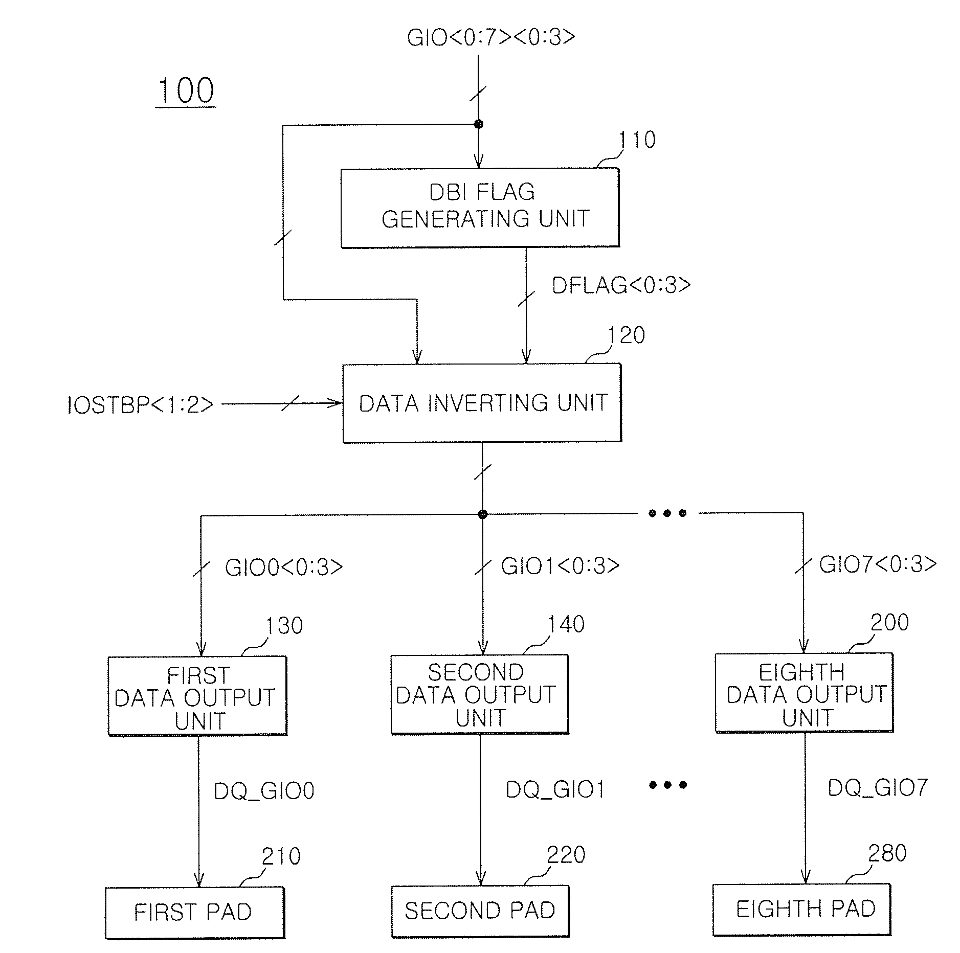
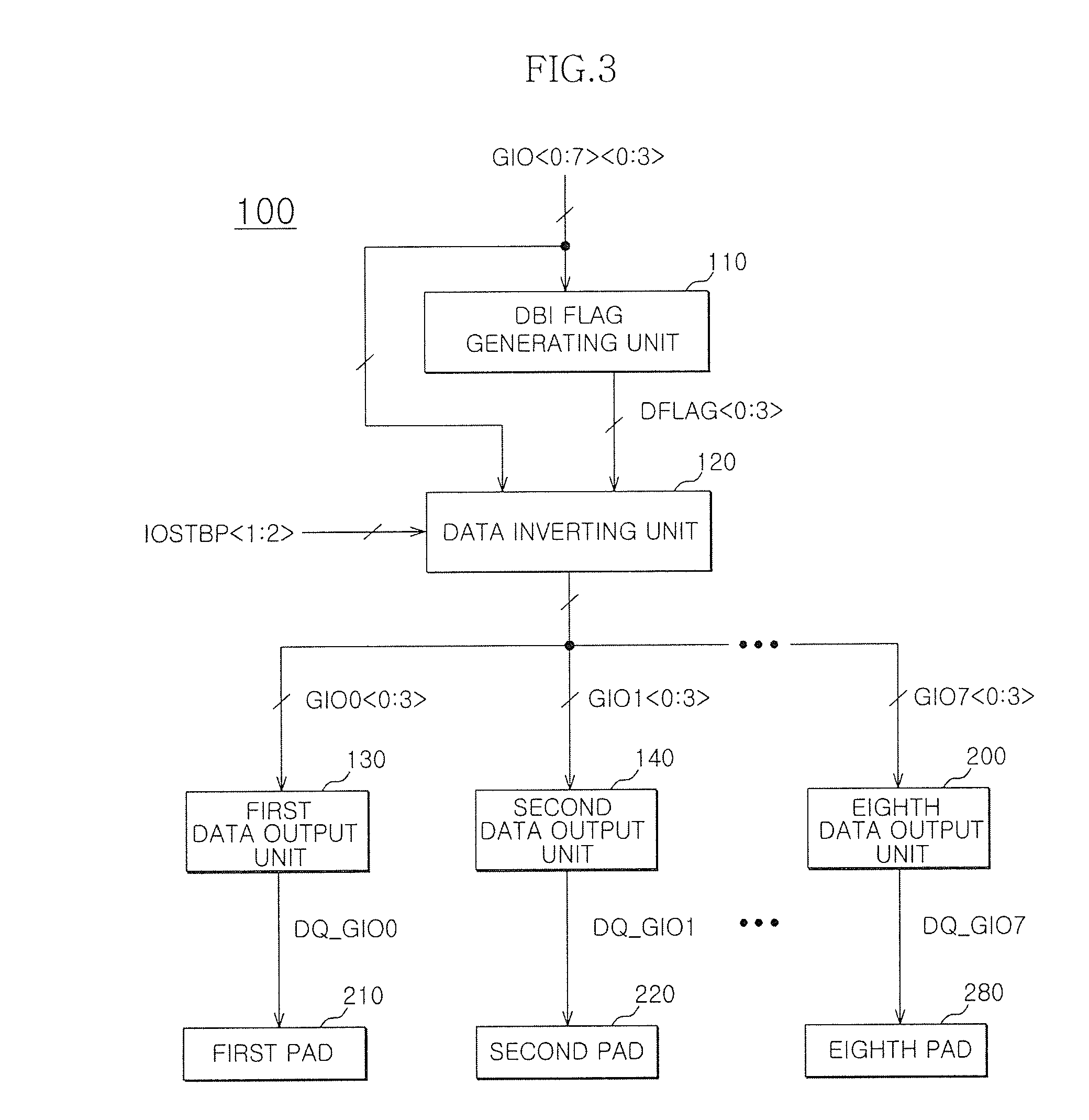
[0031]FIG. 3 is a block diagram showing an exemplary semiconductor integrated circuit device having a data bus inversion function according to an embodiment.

[0032]As shown in FIG. 3, the semiconductor integrated circuit has a data bus inversion function according to an embodiment includes a DBI flag generating unit 110, a data inverting unit 120, first to eighth data output units 130 to 200, and first to eighth pads 210 to 280.

[0033]The DBI flag generating unit 110 performs a predetermined DBI operation on all of data ‘GIO’ output through global transmission lines in a memory cell area (i.e., core block) and generates DBI flag signals ‘DFLAG’ used to define whether data is inverted or not.

[0034]The global transmission lines may be connected between the memory cell area (not shown) and the first to eighth data output units 130 to 200. The data inverting unit 120 may be connected between the global transmission lines.

[0035]The data inverting unit 120 performs a data inversion operatio...


PUM


Abstract

A semiconductor integrated circuit includes a data bus inversion (DBI) flag generating unit to generate DBI flag signals using a plurality of output data sets, a data inverting unit to invert the plurality of output data sets according to the DBI flag signals and transmit the plurality of output data sets through global transmission lines, and a plurality of data output units to output the plurality of output data sets, which are transmitted through the global transmission lines by pads.

Description

CROSS-REFERENCES TO RELATED PATENT APPLICATION[0001]The present application claims priority under 35 U.S.C 119(a) to Korean patent Application No. 10-2008-0112685, filed on Nov. 13, 2008, in the Korean Intellectual Property Office, which is incorporated herein by reference in its entirety.BACKGROUND[0002]The present invention relates generally to a semiconductor integrated circuit (IC) device, and more particularly, to a semiconductor integrated circuit device having a data bus inversion (DBI) function.[0003]FIG. 1 is a block diagram showing a semiconductor integrated circuit (IC) device having a data bus inversion function according to the prior art.[0004]Elements that relate to controlling performance of semiconductor IC devices for storing data are the central processing units (CPU) and / or graphic processing units (GPU). That is, the main memory devices or the graphic memory devices, wherein the data processing speed is one of the most important factors for these devices.[0005]Th...

Claims


Application Information

Patent Timeline
IPC IPC(8): G11C7/00
CPCG11C7/1006G11C7/10G11C7/22
Inventor KWAK, SEUNG WOOK
Owner SK HYNIX INC
Why Eureka
Try Eureka