SRAM and forming method and controlling method thereof
a technology of sram and forming method, which is applied in the field of write operation of an sram, can solve the problems of large negative impact on the write margin of the memory cells of an sram, unreliable performance of the sram, and the inability to maintain the stability of the sram, so as to avoid the failure of write operation, increase the write margin, and adjust the amount of sram cell voltage reduction
- Summary
- Abstract
- Description
- Claims
- Application Information
AI Technical Summary
Benefits of technology
Problems solved by technology
Method used
Image


Examples
Embodiment Construction
[0037]Reference will now be made in detail to the present preferred embodiments of the invention, examples of which are illustrated in the accompanying drawings. Wherever possible, the same reference numbers are used in the drawings and the description to refer to the same or like parts.
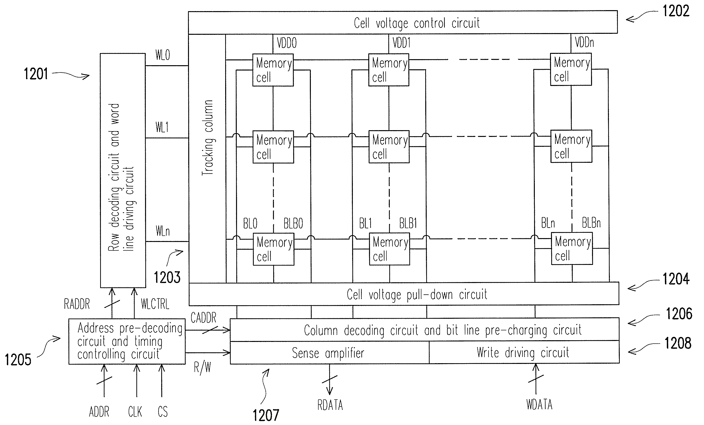
[0038]FIG. 8 is a diagram of a partial circuit of an SRAM according to an embodiment of the present invention. An SRAM in FIG. 8 includes a tracking column 810, a normal column 820, two P-MOSFETs PTK and P0, two N-MOSFETs NTK and N0 and an AND gate 830. The tracking column 810 is designed specifically by the embodiment and has a specific function depicted later on. The tracking column 810 includes a cell power line 811 and a plurality of memory cells (two memory cells are shown in FIG. 8, which the present invention is not limited to). The memory cells of the tracking column 810 receive their cell voltage from the cell power line 811. The normal column 820 is for storing bit data and includes a cell ...
PUM
| Property | Measurement | Unit |
|---|---|---|
| Current | aaaaa | aaaaa |
| Electric potential / voltage | aaaaa | aaaaa |
Abstract
Description
Claims
Application Information