Unlock instant, AI-driven research and patent intelligence for your innovation.

SRAM (static random access memory) and forming method thereof

A memory and storage unit technology, which is applied in the manufacture of electric solid-state devices, semiconductor devices, semiconductor/solid-state devices, etc., can solve the problems of SRAM memory reading and writing stability to be improved, and achieve the effect of reducing complexity and simplifying process steps

Inactive Publication Date: 2012-07-11
SHANGHAI HUAHONG GRACE SEMICON MFG CORP
View PDF6 Cites 1 Cited by
  • Summary
  • Abstract
  • Description
  • Claims
  • Application Information

AI Technical Summary

Problems solved by technology

[0007] Although the performance of the transistors in the storage unit of the existing SRAM memory structure has been improved, the read and write stability of the SRAM memory still needs to be improved

Method used


Image

  • SRAM (static random access memory) and forming method thereof
  • SRAM (static random access memory) and forming method thereof
  • SRAM (static random access memory) and forming method thereof

Examples


Embodiment Construction

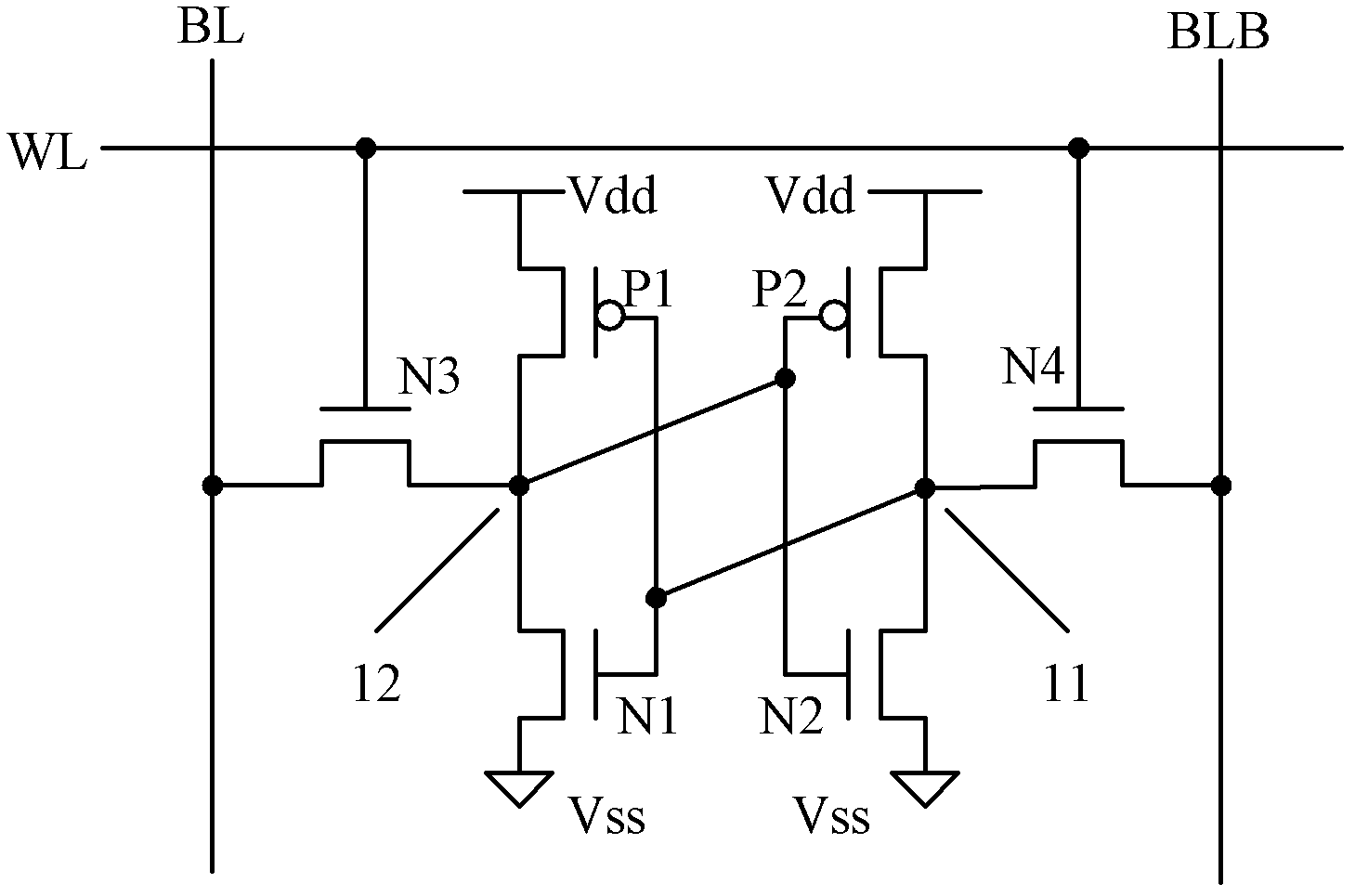
[0045] The read and write stability of SRAM memory is measured by the two parameters of read margin and write margin. Generally speaking, the higher the value of these two parameters, the read and write margin of SRAM memory The better the write stability, where the write margin is the ratio between the saturated source-drain current value of the transfer NMOS transistor and the saturated source-drain current value of the pull-up PMOS transistor; the read margin is the saturated source-drain current value of the pull-down NMOS transistor value to the saturation source-drain current value of the pass NMOS transistor.

[0046] The inventor found in the existing process of manufacturing SRAM memory that the existing SRAM memory forms a tensile stress layer on the surface of the NMOS transistor and a compressive stress layer on the surface of the PMOS transistor, although the transfer of carriers in the NMOS transistor and the PMOS transistor can be improved rate, but the improvem...


PUM

PropertyMeasurementUnit
Thicknessaaaaaaaaaa
Stressaaaaaaaaaa

Abstract

The invention relates to a SRAM (static random access memory) and a forming method thereof. The SRAM memory comprises: a substrate, a plurality of memory cells arranged on the substrate in line, and tensile stress layers, wherein each memory cell comprises at least one NMOS (N-channel mental oxide semiconductor) transistor and a PMOS (P-channel metal oxide semiconductor) transistor; the tensile stress layers are located on the surfaces of the NMOS transistor, the PMOS transistor and the substrate. The SRAM memory of the embodiment of the invention increase the writing tolerance while keeping the reading tolerance constant and the process complexity is reduced by the forming method of the SRAM memory.

Description

technical field [0001] The invention relates to the field of semiconductor manufacturing, in particular to an SRAM memory and a forming method thereof. Background technique [0002] Static random access memory (SRAM), as a member of volatile memory, has the advantages of high speed, low power consumption and compatibility with standard processes, and is widely used in PCs, personal communications, consumer electronics (smart cards, digital cameras, multimedia players ) and other fields. [0003] figure 1 It is a schematic diagram of the circuit structure of the storage unit of the existing 6T structure SRAM memory, the storage unit includes: a first PMOS transistor P1, a second PMOS transistor P2, a first NMOS transistor N1, a second NMOS transistor N2, and a third NMOS transistor N3 and the fourth NMOS transistor N4, the first PMOS transistor P1, the second PMOS transistor P2, the first NMOS transistor N1, and the second NMOS transistor N2 form a bistable circuit, and the...

Claims


Application Information

Patent Timeline
IPC IPC(8): H01L27/11H01L21/8244
Inventor 胡剑孔蔚然
Owner SHANGHAI HUAHONG GRACE SEMICON MFG CORP