Method for making nanowire structure
a nanowire and nanofiber technology, applied in the direction of electrical equipment, metallic material coating process, chemical vapor deposition coating, etc., can solve the problems of high voltage, complex equipment, and high cost of electroplating method for fabricating titanium dioxide nanofibers, and achieve the effect of reducing the cost of electroplating
- Summary
- Abstract
- Description
- Claims
- Application Information
AI Technical Summary
Benefits of technology
Problems solved by technology
Method used
Image
Examples
example 1
Method for Manufacturing TiO2 Nanowires
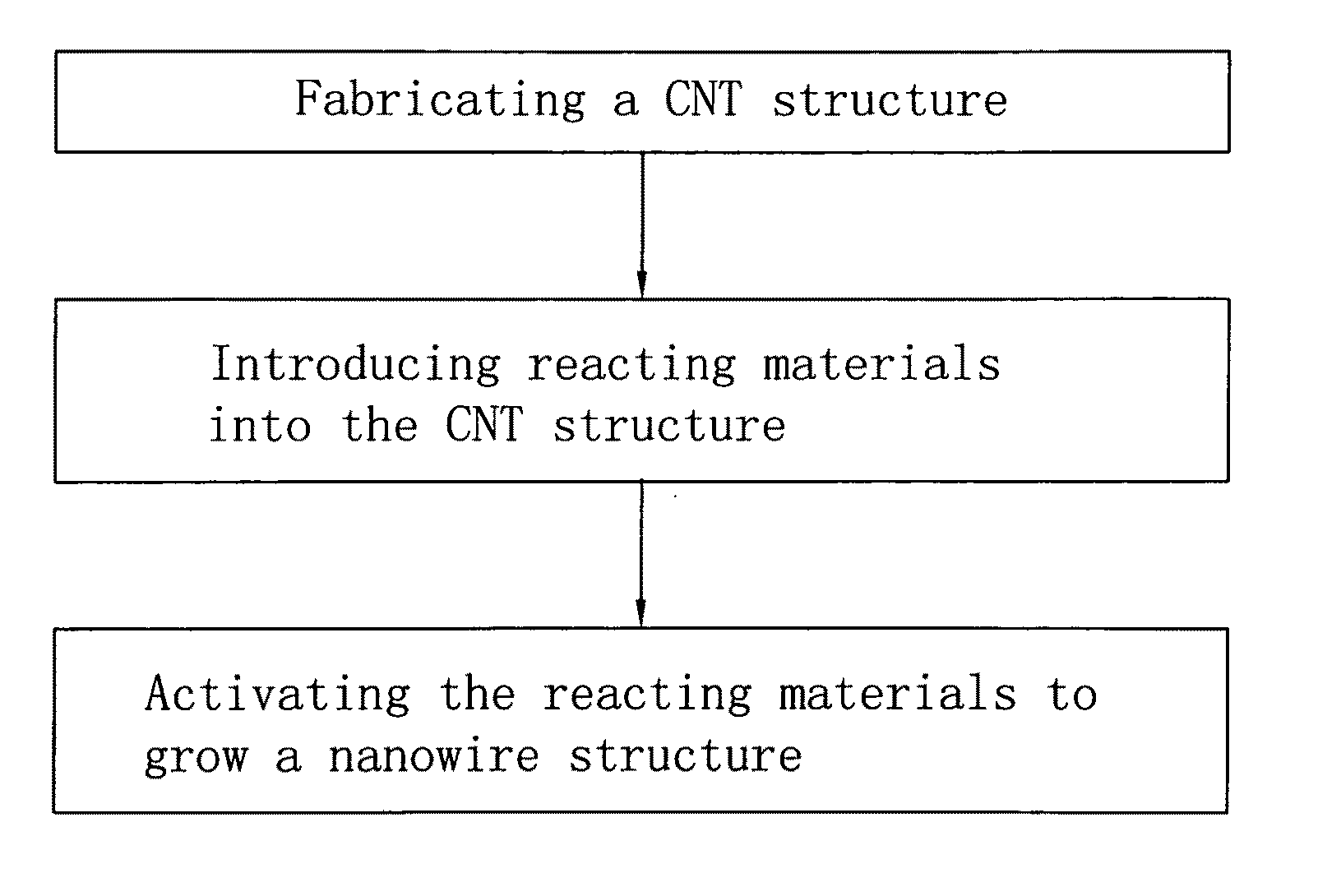
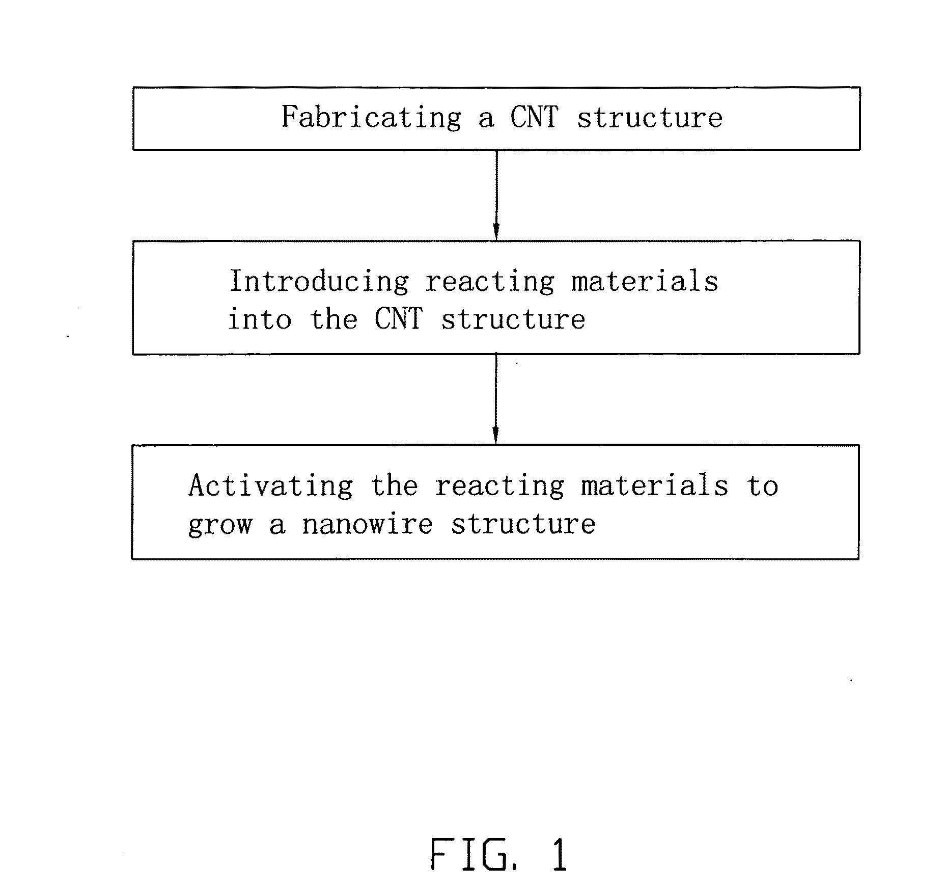
[0069]Referring to FIG. 9, in a first embodiment, a method of fabricating a TiO2 nanowire structure 104 includes (a1) providing a two dimension carbon nanotube structure 100, (a2) introducing reacting materials 102 into the carbon nanotube structure 100, and (a3) activating the reacting materials 102 to grow the TiO2 nanowires structure 104.
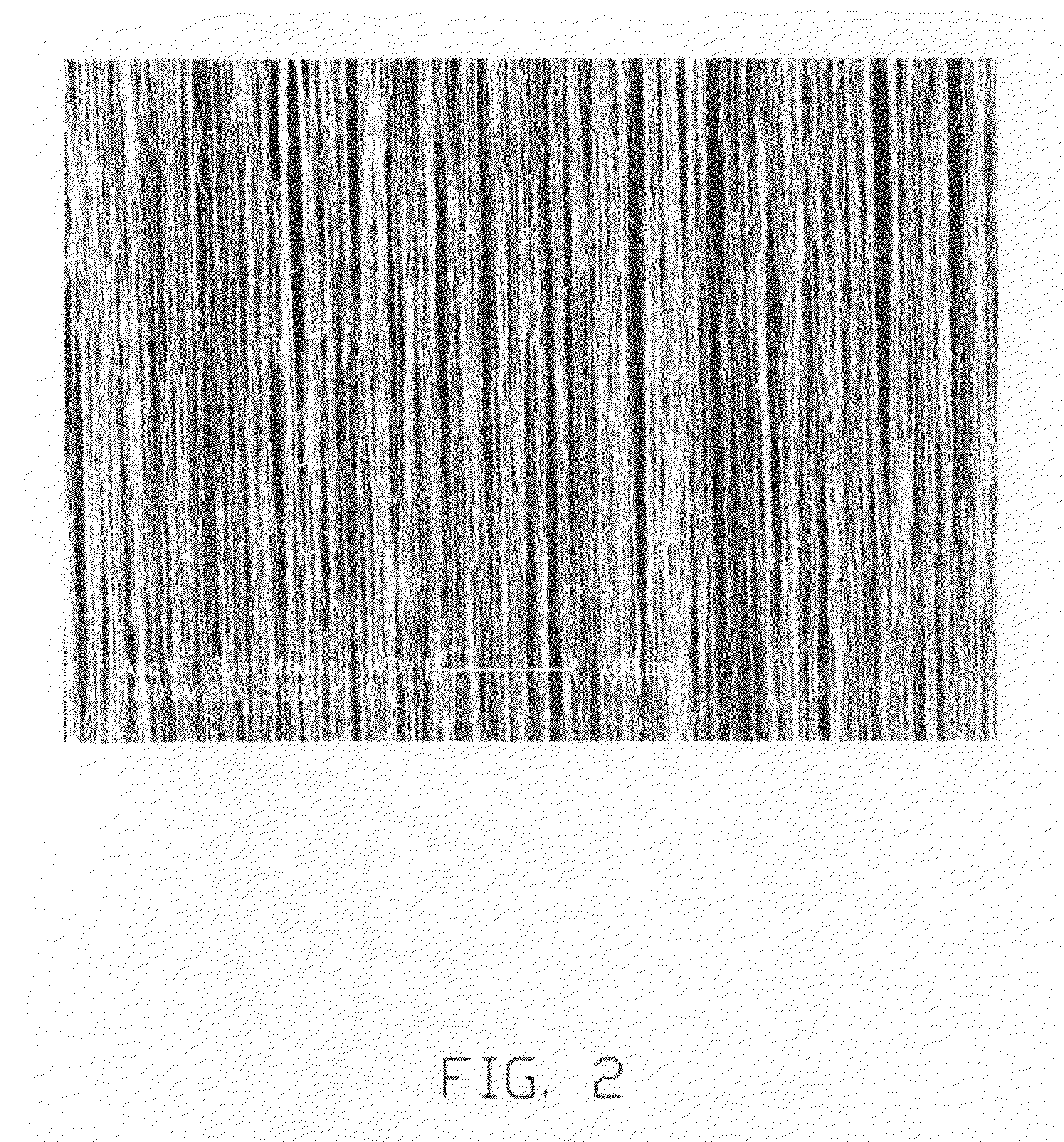
[0070]In step (a1), the two dimension carbon nanotube structure 100 is obtained by stacking two drawn carbon nanotube films. The carbon nanotubes of the drawn carbon nanotube film are oriented substantially along the same direction.
[0071]In step (a2), a 100 nm thick titanium layer as reacting material 102 is sputtered on the carbon nanotube structure 100 by the magnetron sputtering method. Referring to FIGS. 10-12, the titanium particles of the titanium layer are uniformly distributed on the surface of the drawn carbon nanotube film.
[0072]In step (a3), the carbon nanotube structure 100 is placed in an atmosp...
example 2
Method for Manufacturing TiO2 Nanowires
[0074]Referring to FIG. 14, in a second embodiment, a method of fabricating a TiO2 nanowire structure 204 is similar to the first embodiment, differing only in the use of two stacked drawn carbon nanotube films. The discernable angle between two adjacent carbon nanotube films is about 90°.
[0075]The method of fabricating the TiO2 nanowire nanostructure 204 includes (b1) providing a two dimension carbon nanotube structure 200, (b2) introducing reacting materials 202 into the carbon nanotube structure 200, and (b3) activating the reacting materials 202 to grow the TiO2 nanowire nanostructure 204.
[0076]In step (b1), the two dimension carbon nanotube structure 200 is obtained by stacking two drawn carbon nanotube films. The carbon nanotubes of the two drawn carbon nanotube films are oriented along different directions. The discernable angle between two adjacent drawn carbon nanotube films is about 90°.
[0077]In step (b2), the reacting materials 202 a...
example 3
Method for Manufacturing TiO2 Nanowires
[0079]Referring to FIG. 16, in a third embodiment, a method of fabricating a TiO2 nanowires structure 304 is similar to the first embodiment, differing only in the use of at least one carbon carbon nanotube wire as a template.
[0080]A method of fabricating the TiO2 nanowires structure 304 includes the following steps of (c1) providing a one dimensional carbon nanotube structure 300, (c2) introducing reacting materials 302 into the carbon nanotube structure 300, and (c3) activating the reacting materials 302 to grow the TiO2 nanowires structure 304.
[0081]In step (c1), the one dimensional carbon nanotube structure 300 can be one carbon nanotube wire or a plurality of carbon nanotube wires substantially parallel to each other. The diameter of the carbon nanotube wire is less than 100 nm. In one embodiment, the one dimensional carbon nanotube structure 300 includes a plurality of the carbon nanotube wire bundled together. Gaps of these carbon nanotu...
PUM
| Property | Measurement | Unit |
|---|---|---|
| angle | aaaaa | aaaaa |
| thickness | aaaaa | aaaaa |
| thickness | aaaaa | aaaaa |
Abstract
Description
Claims
Application Information


