
Semiconductor integrated circuit device

Active Publication Date: 2010-05-27
ABLIC INC
View PDF1 Cites 2 Cited by
  • Summary
  • Abstract
  • Description
  • Claims
  • Application Information

AI Technical Summary

Benefits of technology

[0030]According to the present invention, a semiconductor integrated circuit device including an analog circuit which has a small variation in characteristic of each MOS transistor and is reduced in size and cost may be provided.

Problems solved by technology

Differences among the characteristics generate an offset voltage in the operational amplifier and a current error in the current mirror circuit, giving possible degradation to the product characteristics itself.
In particular, when the scale of the analog signal processing circuit becomes larger, the trade-off becomes significant, and hence it is difficult to obtain benefits from a miniaturization technology used for a digital signal processing circuit.
In addition, in a case of a digital and analog mixed IC, a process combination between them may also be limited in some cases.
However, the conventional well region formation method using the semiconductor process as described above has the following problem.
Thus, the MOS transistors arranged close to the boundary regions, in particular, the P-channel MOS transistor located on the N-type well region side has a problem that it is more likely to cause the variation in characteristic due to the change in concentration.

Method used


Image

  • Semiconductor integrated circuit device
  • Semiconductor integrated circuit device
  • Semiconductor integrated circuit device

Examples


first embodiment

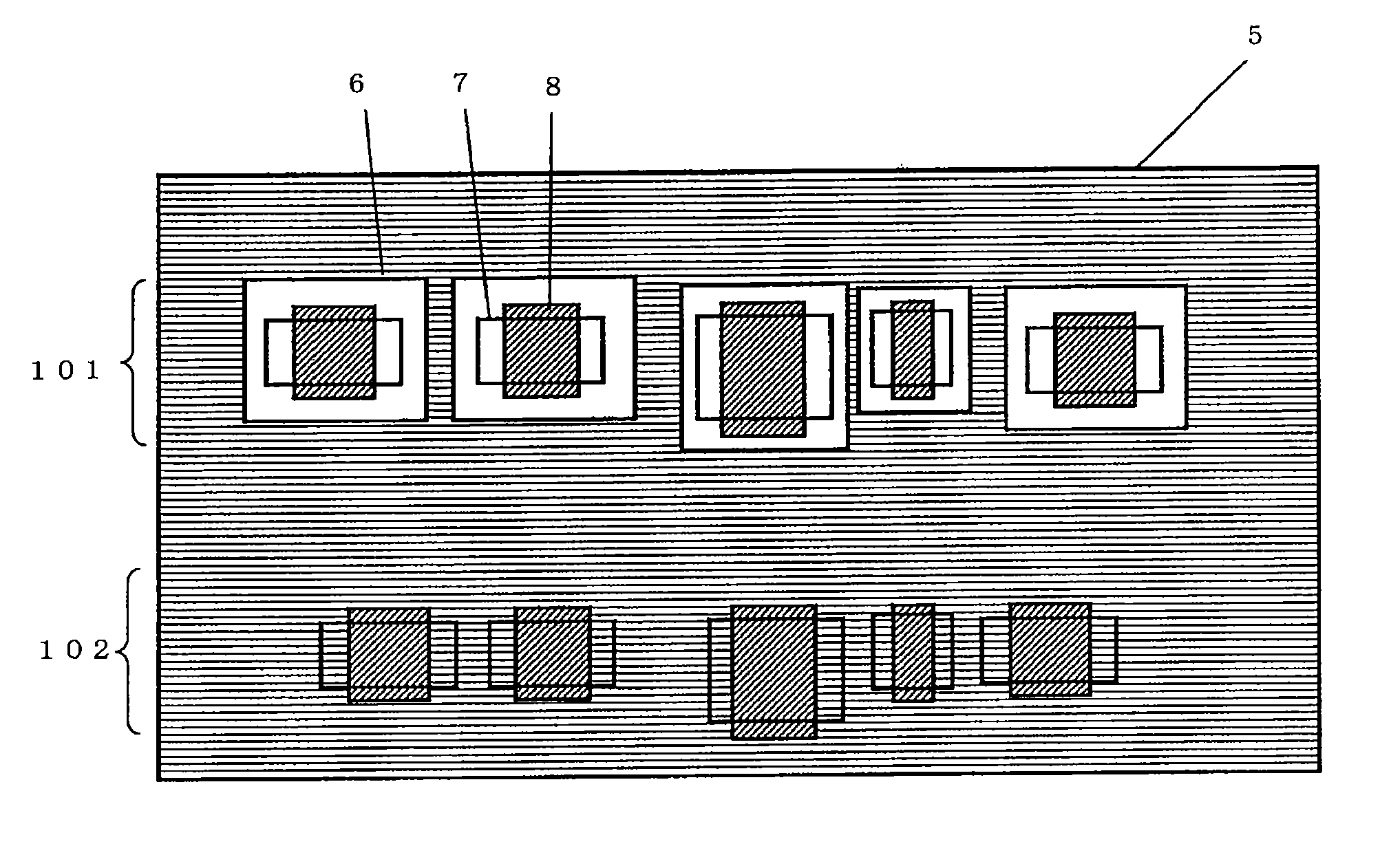
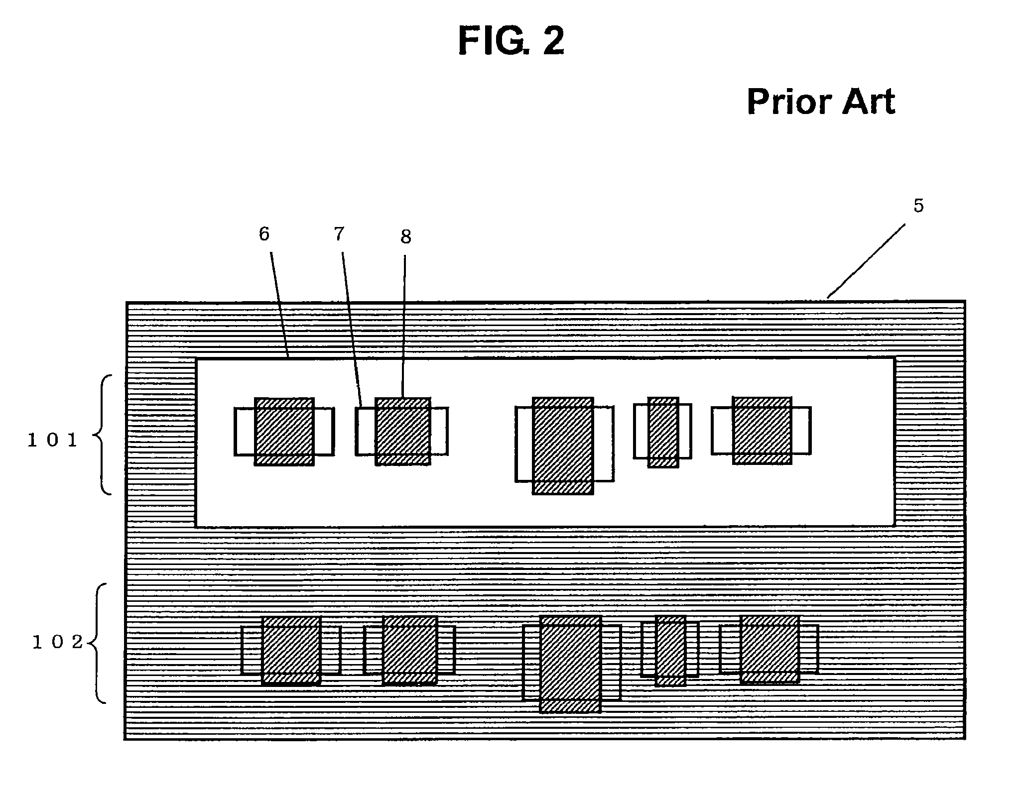
[0037]Hereinafter, embodiments of the present invention are described with reference to the attached drawings. FIG. 1 is a schematic plan view illustrating a semiconductor integrated circuit device in which a variation in characteristics of MOS transistors is reduced, according to the present invention. In FIG. 2 illustrating the conventional method, the plurality of P-channel MOS transistors 101 are arranged within the single N-type well region 6. In contrast to this, according to the present invention, a single P-channel MOS transistor 101 is provided within each of N-type well regions 6. The provided P-channel MOS transistors 101 serve as a circuit block. In this case, all the P-channel MOS transistors 101 are adjusted such that distances between channel regions and edges of the N-type well regions 6 under polysilicon gate electrodes 8 are equal to one another. When the enlarged view of FIG. 4A is referred to, the distance between the channel region and the N type well region is ...

second embodiment

[0042]FIG. 5 is a schematic plan view illustrating a semiconductor integrated circuit device according to the present invention. In this embodiment, as in the case of the N-type well regions located in the P-type semiconductor substrate, the respective P-type well regions are provided for corresponding N-channel MOS transistors. In order to realize this, a single N-channel MOS transistor 102 is formed on each of P-type well regions 5. An N-type well region 6 is formed to surround the P-type well regions, to thereby set boundary regions.

[0043]The layout as illustrated in FIG. 5 is useful for not only the P-channel MOS transistors but also the N-channel MOS transistors in the analog circuit required to have a high-precision relative ratio between adjacent transistors.

[0044]That is, any MOS transistor to which the present invention is applied may be freely selected based on a circuit type such as an analog circuit type or a digital circuit type and required precision during design and ...


PUM


Abstract

Provided is a semiconductor integrated circuit device capable of realizing an analog circuit required to have a high-precision relative ratio between adjacent transistors, which is reduced in size and cost. A single MOS transistor is provided within each of well regions. A plurality of the MOS transistors is combined to serve as an analog circuit block. Since distances between the well regions and channel regions may be made equal to one another, a high-precision semiconductor integrated circuit device can be obtained.

Description

RELATED APPLICATIONS[0001]This application claims priority under 35 U.S.C. §119 to Japanese Patent Application No. JP2008-300715 filed Nov. 26, 2008, the entire content of which is hereby incorporated by reference.BACKGROUND OF THE INVENTION[0002]1. Field of the Invention[0003]The present invention relates to a semiconductor integrated circuit device including an analog signal processing circuit having MOS transistors.[0004]2. Description of the Related Art[0005]In a semiconductor integrated circuit, in particular, in an analog signal processing circuit, which includes MOS transistors, difference in characteristics between adjacent MOS transistors is required to be small enough. The analog signal processing circuit includes an operational amplifier and a current mirror circuit, and has a function of producing a plurality of current sources with a certain ratio to compare and amplify a plurality of voltages with high precision. Having the same structure and layout the MOS transistors...

Claims


Application Information

Patent Timeline
IPC IPC(8): H01L27/088
CPCH01L21/823892H01L27/0928H01L27/0207
Inventor HARADA, HIROFUMI
Owner ABLIC INC
Features
  • Generate Ideas
  • Intellectual Property
  • Life Sciences
  • Materials
  • Tech Scout
  • Unparalleled Data Quality
  • Higher Quality Content
  • 60% Fewer Hallucinations
Learn More