Thin Film Silicon Solar Cell Device With Amorphous Window Layer

a solar cell and thin film technology, applied in the field of thin film silicon solar cell devices with amorphous window layers, can solve the problems of 15-20% loss of starting efficiency

Inactive Publication Date: 2010-06-03
APPLIED MATERIALS INC
View PDF4 Cites 69 Cited by
  • Summary
  • Abstract
  • Description
  • Claims
  • Application Information

AI Technical Summary

Benefits of technology

[0008]One embodiment of the present invention relates to a photovoltaic device, comprising a micro-crystal, thin film silicon solar cell comprising an absorber layer comprising micro-crystal silicon having a bandgap; and a window layer adjacent the absorber layer, the window layer comprising a material with a higher bandgap than the micro-crystal silicon. In one embodiment, the window layer comprises amorphous silicon. In one embodiment, the window layer comprises carbon-doped silicon (Si:C). In one embodiment, the emitter layer has a bandgap of about or greater than 1.3 eV.

Problems solved by technology

This type of cell, because of defects in the crystal structure, may suffer from a light-induced degradation which is known as the Stabler-Wronski effect, which may result in a loss of 15-20% of its starting efficiency.

Method used


Image

  • Thin Film Silicon Solar Cell Device With Amorphous Window Layer
  • Thin Film Silicon Solar Cell Device With Amorphous Window Layer
  • Thin Film Silicon Solar Cell Device With Amorphous Window Layer

Examples


Embodiment Construction

[0024]Embodiments of the invention generally provide photovoltaic devices and methods of forming and treating photovoltaic devices. Before describing several exemplary embodiments of the invention, it is to be understood that the invention is not limited to the details of construction or process steps set forth in the following description. The invention is capable of other embodiments and of being practiced or being carried out in various ways.

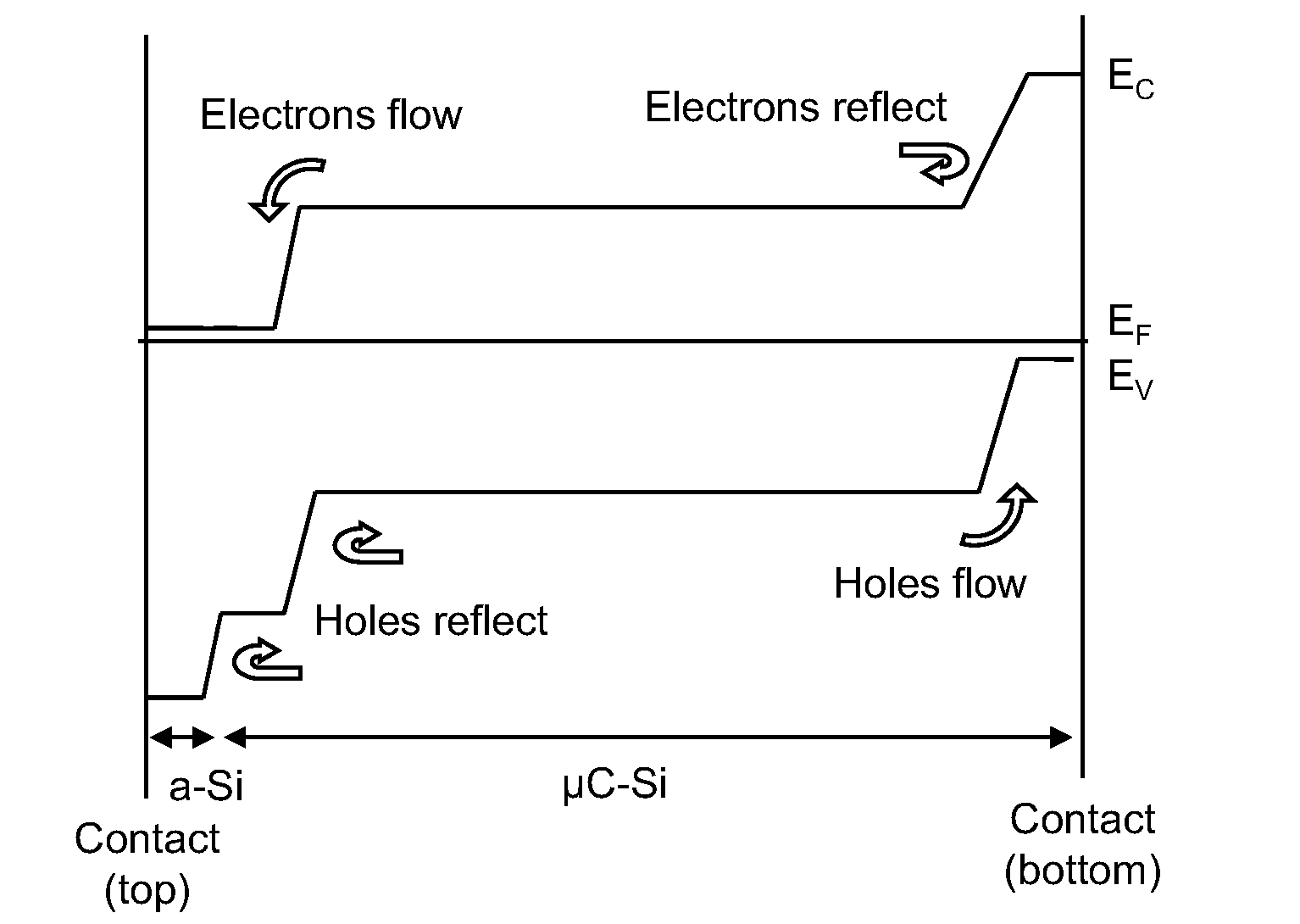
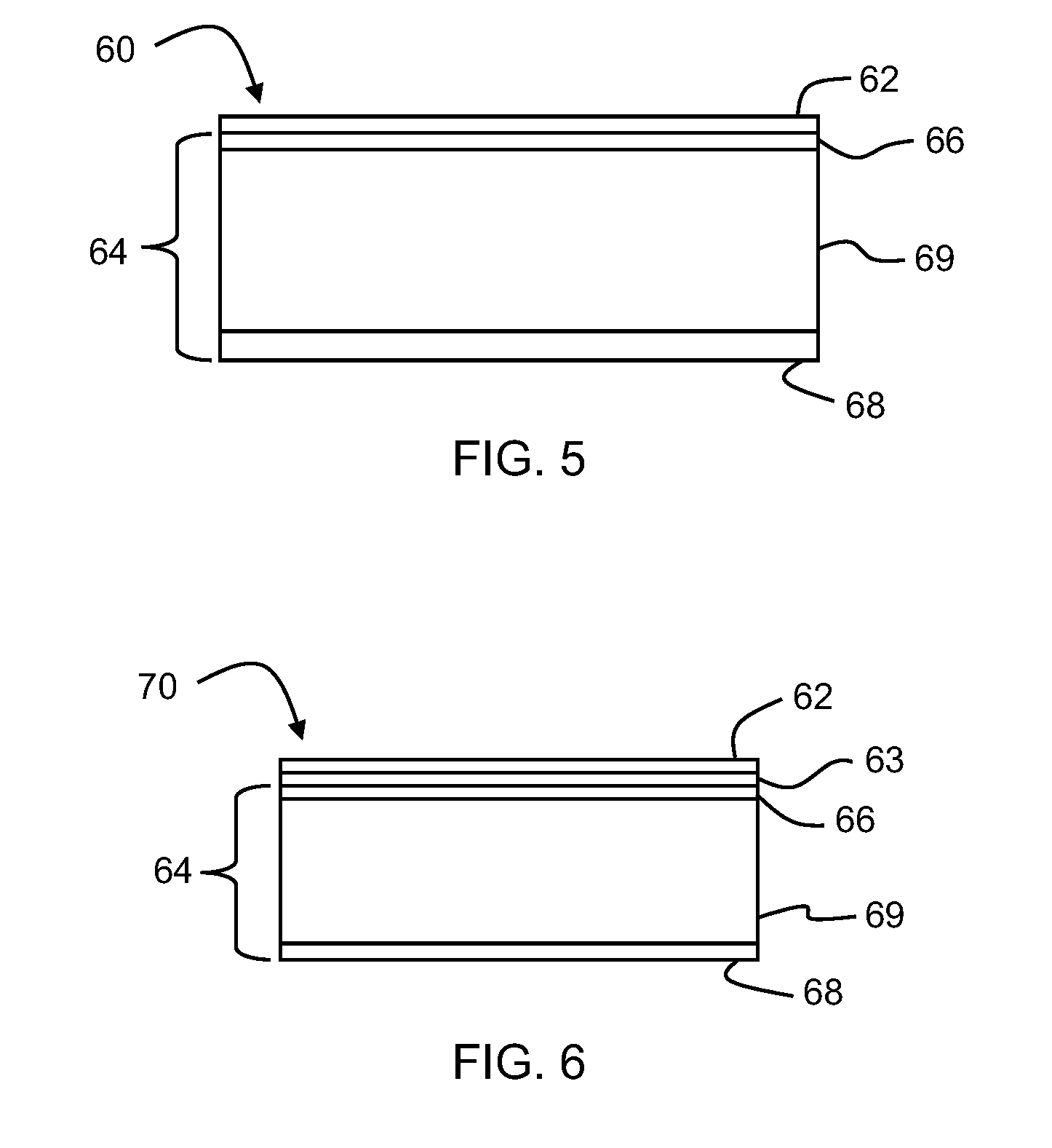
[0025]According to one embodiment of the invention, a photovoltaic device 60 comprises a layer of amorphous silicon (“a-Si”) 62 formed over a μC-Si solar cell 64, as shown in FIG. 5. In one embodiment, the a-Si is substantially pure. In other embodiments, the μC-Si 68 is doped to a first conductivity type and the a-Si layer 62 may be doped to the opposite conductivity type of the μC-Si (i.e., the same type as the emitter of the μC-Si cell) as is shown in FIG. 5. As shown in FIG. 5, the μC-Si solar cell 64 comprises an optional first micro-cry...


PUM

PropertyMeasurementUnit
thicknessaaaaaaaaaa
conductivity typeaaaaaaaaaa
conductivityaaaaaaaaaa

Abstract

Photovoltaic devices and methods of manufacture are provided. In an embodiment, the devices comprise a micro-crystal silicon cell having an amorphous silicon layer formed on the micro-crystal cell.

Description

FIELD[0001]Embodiments of the present invention generally relate to photovoltaic (PV) devices and fabrication of photovoltaic devices. In particular, embodiments of the invention relate to amorphous silicon window layer on micro-crystal silicon and creation thereof in photovoltaic devices.BACKGROUND[0002]Thin film silicon solar cells for photovoltaic purposes are known. The silicon in a solar device may be classified according to its crystallinity. Commonly used classification of silicon crystallinity include: single-crystalline, polycrystalline, microcrystalline (micro-crystal) and amorphous. An amorphous silicon cell 10 shown in cross-sectional diagram in FIG. 1 may be considered one of the least complex of the silicon solar cell structures. It has a thin (100-200 Å thick) p-type layer 12 and an n-type silicon layer 14 that sandwich a low-doped intrinsic layer 16 on the order of 3000 Å thick. This type of cell, because of defects in the crystal structure, may suffer from a light-i...

Claims


Application Information

Patent Timeline
Patent Type & Authority Applications(United States)
IPC IPC(8): H01L31/00H01L31/0232
CPCH01L31/03685Y02E10/545Y02E10/548H01L31/075
Inventor BORDEN, PETER G.
Owner APPLIED MATERIALS INC
Why Eureka
Try Eureka