

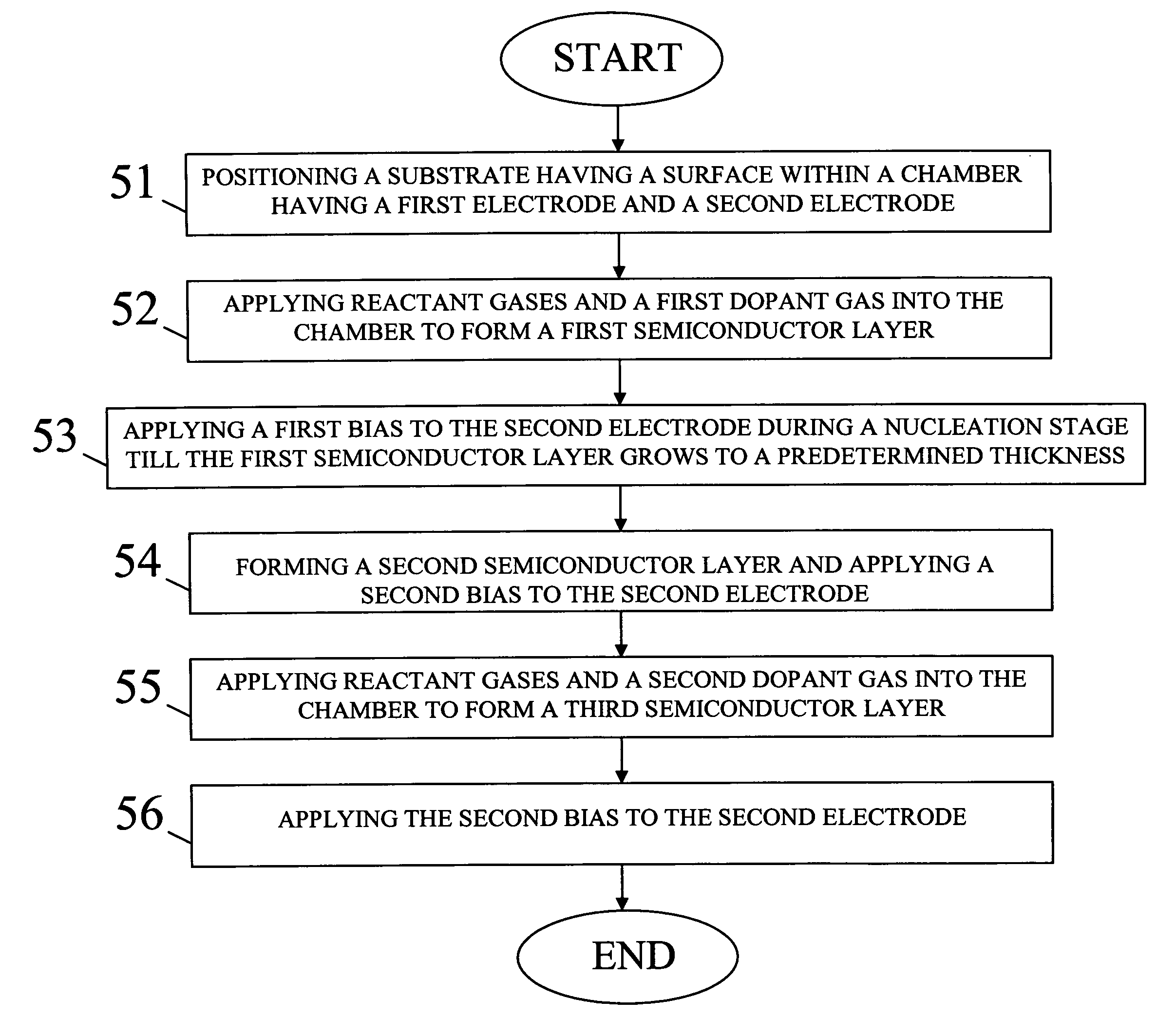
Method of forming microcrystalline silicon film
a microcrystalline silicon and film technology, applied in the field of semiconductor fabrication, can solve the problems of c-based cells, relatively high electricity generation cost of wafer-type solar cells,
- Summary
- Abstract
- Description
- Claims
- Application Information
AI Technical Summary
Benefits of technology
Problems solved by technology
Method used
Image

Examples
Embodiment Construction
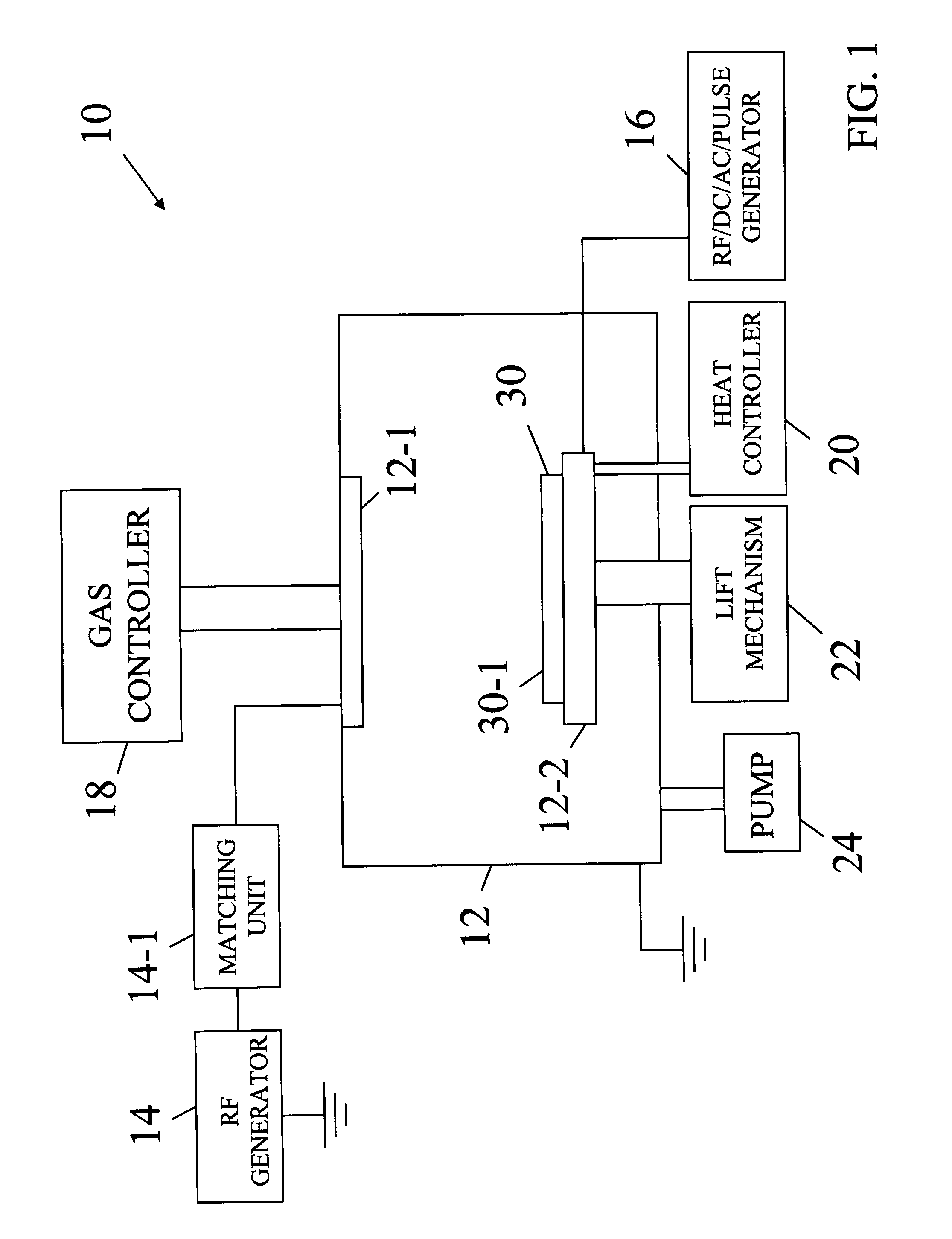
[0018]FIG. 1 is a schematic diagram of a system 10 capable of forming a microcrystalline silicon (μc-Si) film consistent with an example of the present invention. The μc-Si film or nanocrystalline silicon film may refer to a polycrystalline silicon film having a grain size ranging from approximately 10 to 100 nanometer (nm). However, the range may be different in particular applications. The system 10 in other examples may also be capable of forming microcrystalline silicon carbide (μc-SiC), microcrystalline silicon germanium (μc-SiGe), amorphous silicon and amorphous silicon germanium (a-SiGe). Referring to FIG. 1, the system 10 may include a chamber 12, a first power generator 14 and a second power generator 16. As an example, the system 10, except the second power generator 16, may include a model AKT-1600 plasma-enhanced chemical vapor deposition (PECVD) system manufactured by Applied Komatsu Technology, a high density plasma CVD (HDPCVD) system manufactured by Applied Materials...
PUM
 Abstract
Description
Claims
Application Information