Preparation method of double-sided passivated crystalline silicon solar cell

A solar cell, double-sided passivation technology, applied in circuits, electrical components, semiconductor devices, etc., can solve the problem of unsuitable P-type silicon wafer surface passivation, etc., to improve thermal stability, output performance, and process window. big effect

Inactive Publication Date: 2011-01-05
SHANGHAI JIAO TONG UNIV
View PDF5 Cites 32 Cited by
  • Summary
  • Abstract
  • Description
  • Claims
  • Application Information

AI Technical Summary

Problems solved by technology

At present, the commonly used passivation technology is to use plasma-enhanced chemical vapor deposition system to prepare silicon nitride film or silicon oxide passivation film. These films are rich in high-density positive charges and are suitable for passivating N-type silicon wafers. Surface passivation of P-type silicon wafer

Method used


Image

  • Preparation method of double-sided passivated crystalline silicon solar cell
  • Preparation method of double-sided passivated crystalline silicon solar cell
  • Preparation method of double-sided passivated crystalline silicon solar cell

Examples


Embodiment

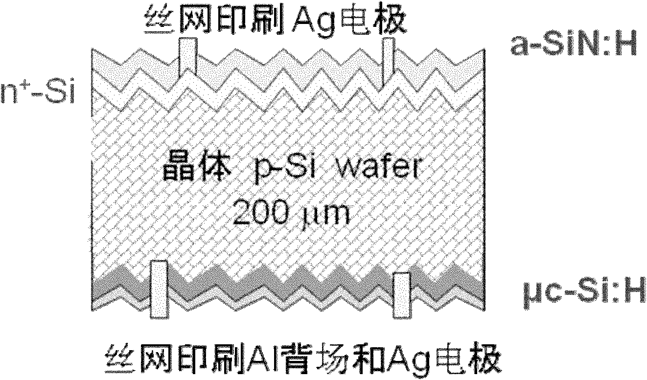
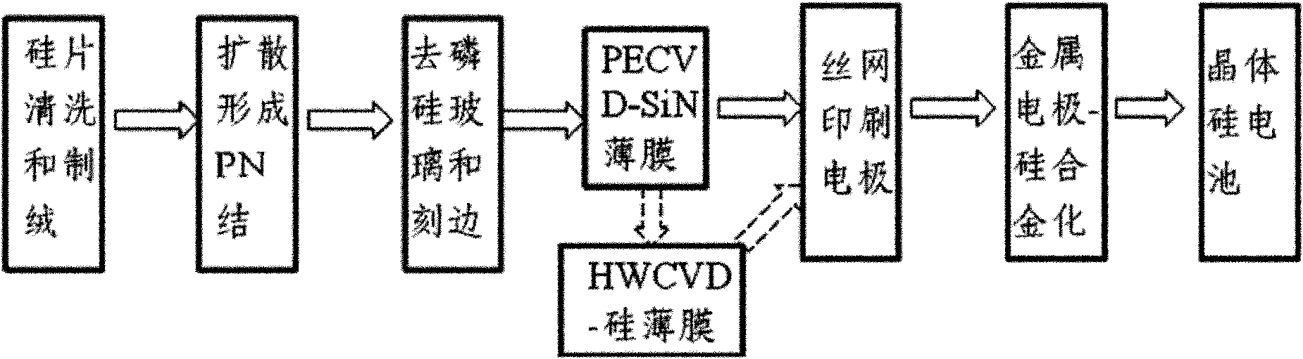
[0032] ①The surface of P-type monocrystalline silicon wafer is pre-cleaned and surface textured by semiconductor cleaning process. The thickness of the silicon wafer used is about 200μm, and the area is 125x125mm 2 Quasi-square sheet, resistivity 1Ω·cm, use about 1-5% hydrofluoric acid to remove SiO on the surface of silicon sheet 2 layer. Next, a pyramid-shaped textured surface is prepared on the P-type single crystal silicon wafer in a mixed solution of NaOH and isopropanol (IPA) with a concentration of less than 3% at about 80°C. It was then ultrasonically cleaned with deionized water and blown dry with nitrogen.

[0033] ②Use a tubular diffusion furnace, use phosphorus oxychloride as the diffusion source, and nitrogen as the source gas to diffuse phosphorus on the p-type monocrystalline silicon wafer after texturing to form an N-type emission layer, thereby forming a PN junction, in which the emission Area square resistance 30-80Ω / □.

[0034] ③ Use HF solution with a c...


PUM

PropertyMeasurementUnit
thicknessaaaaaaaaaa
electrical resistivityaaaaaaaaaa
particle sizeaaaaaaaaaa

Abstract

The invention discloses a preparation method of a double-sided passivated crystalline silicon solar cell, belonging to the technical field of photovoltaic power generation. The preparation method comprises the following steps of: firstly, respectively carrying out surface precleaning and surface texturing on P-shaped single crystal silicon and a polycrystalline silicon wafer by adopting an alkaline solution and an acid solution; secondly, diffusing by using phosphorus oxychloride as a diffusion source to form a PN junction; thirdly, removing a phosphosilicate glass on the surface of the silicon wafer by adopting a chemical wet method, and etching the edge of the silicon wafer by adopting a plasma; fourthly, preparing a silicon nitride film on the surface of an emitting region of a P-type silicon wafer by adopting a plasma enhanced chemical vapor deposition method; fifthly, preparing a mixed phase film material of hydrogenated microcrystalline silicon and amorphous silicon by adopting a hot filament chemical vapor deposition method, depositing a film at one side of the P-type silicon wafer, and passivating the defects and a dangling bond on the surface of the P-type silicon wafer; and sixthly, sintering a screen printing back electrode and a screen printing positive electrode to form the solar cell. The invention lowers the probability of compounding photo-generated minority carriers on the back surface, enhances the long-wave light quantum efficiency and creates the conditions of transportation and collection of the photo-generated carriers.

Description

technical field [0001] The patent of the present invention relates to a preparation method in the technical field of photovoltaic power generation, in particular to a preparation method of double-sided passivated crystalline silicon solar cells. Background technique [0002] The solar photovoltaic power generation industry has developed very rapidly. Since 2007, China's photovoltaic production has been the first in the world. The product types are mainly crystalline silicon cells and modules, accounting for nearly 90% of the market share, and thin-film cells account for about 10% of the market. Although China's photovoltaic manufacturing volume ranks first, the photoelectric conversion efficiency of photovoltaic products is at a medium level and lacks core technologies. To enhance the core competitiveness of photovoltaic products in the global market, it is necessary to develop new technologies, improve the photoelectric conversion capabilities of photovoltaic cells and modu...

Claims


Application Information

Patent Timeline
Patent Type & Authority Applications(China)
IPC IPC(8): H01L31/18
Inventor 孟凡英张松汪建强韩涛程雪梅司新文李翔黄建华
Owner SHANGHAI JIAO TONG UNIV
Why Eureka
Try Eureka