

Photovoltaic device
a photovoltaic device and photovoltaic technology, applied in the field of photovoltaic devices, can solve the problems of resistivity and transmittance decreasing, resistivity and transmittance reducing, and it is difficult to achieve the desired aspects of resistivity and transmittance, so as to prevent the transmission of the transparent electrode from being decreased, enhance the transmission, and increase the transmittance
- Summary
- Abstract
- Description
- Claims
- Application Information
AI Technical Summary
Benefits of technology
Problems solved by technology
Method used
Image

Examples
first embodiment
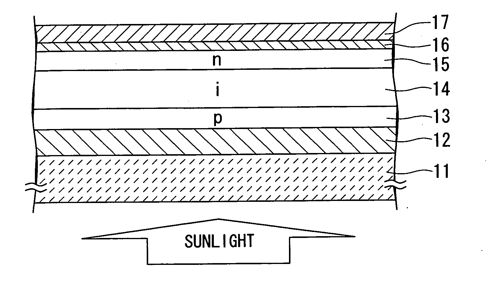
[0060] A photovoltaic device according to a first embodiment of the present invention is described with reference to FIG. 1.
[0061] The photovoltaic device according to the first embodiment includes electricity-generating layers made of microcrystalline silicon and receives incident light via an electrically insulating transparent substrate.
First Step
[0062] A first transparent electrode 12 is formed on an electrically insulating transparent substrate 11 optically transparent white crown glass, for example, can be used for the electrically insulating transparent substrate 11.
[0063] The first transparent electrode 12 is made of zinc oxide (ZnO) doped with gallium (Ga). Furthermore, an antireduction film may be formed on the first transparent electrode 12.
[0064] The electrically insulating transparent substrate 11 is housed in a DC sputtering apparatus, and a Ga-doped ZnO layer is formed on the transparent electrically insulating substrate 11 by evacuating the reaction chamber to ...
second embodiment
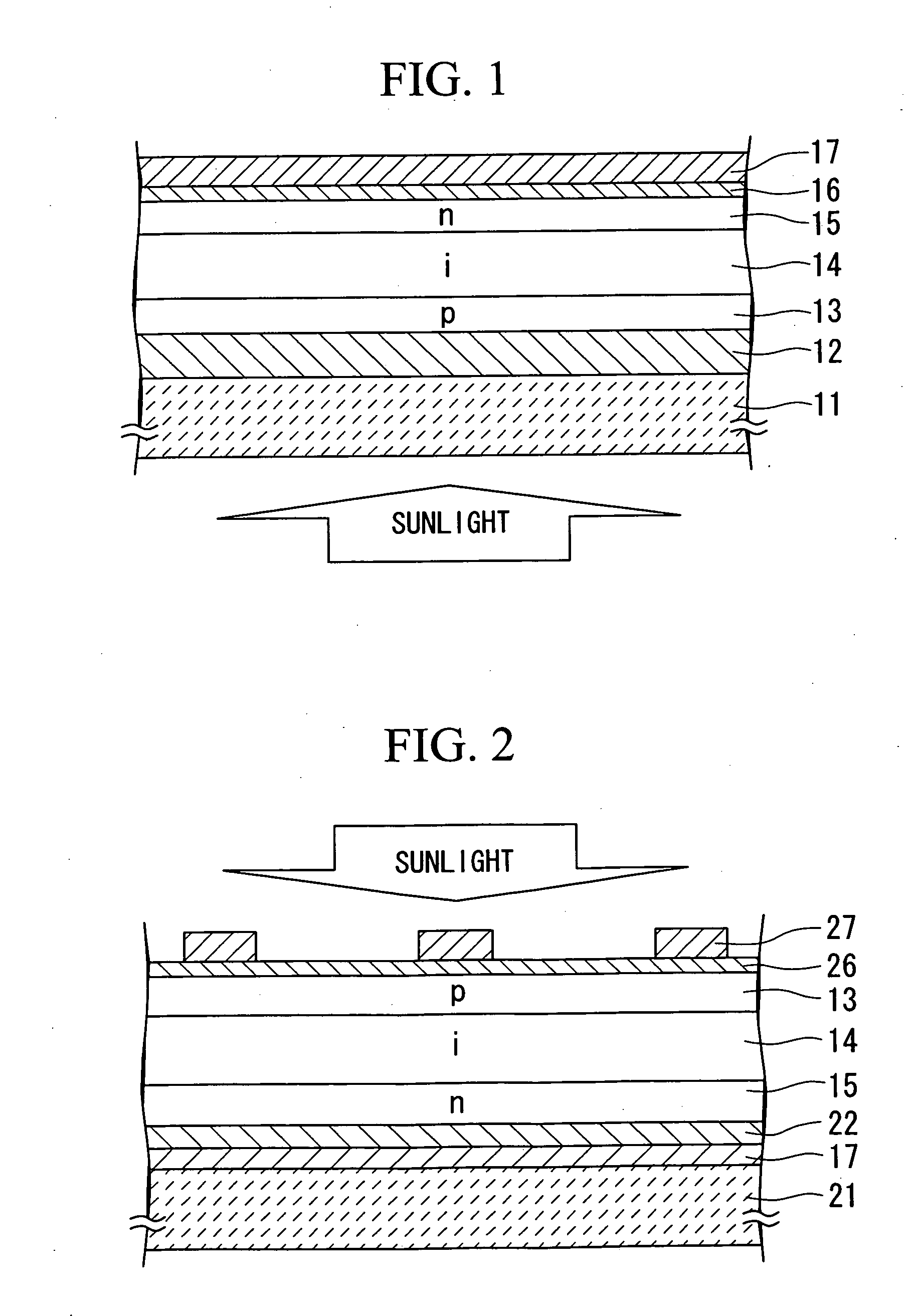
[0086] A photovoltaic device according to a second embodiment of the present invention is described with reference to FIG. 2.
[0087] The photovoltaic device according to the second embodiment is similar to the photovoltaic device according to the first embodiment in that electricity-generating layers are made of microcrystalline silicon. Unlike the photovoltaic device according to the first embodiment, the photovoltaic device according to the second embodiment is constructed so as to receive incident light via an opposite collecting electrode to enable an electrically insulating opaque substrate to be used.
First Step
[0088] A back electrode 17 and a first transparent electrode 22 are formed on an electrically insulating opaque substrate 21 that does not transmit light. A stainless steel plate, for example, is used as the electrically insulating opaque substrate 21. Soda-lime glass may be used in place of the electrically insulating opaque substrate 21.
[0089] For example, Ag or Al...
third embodiment
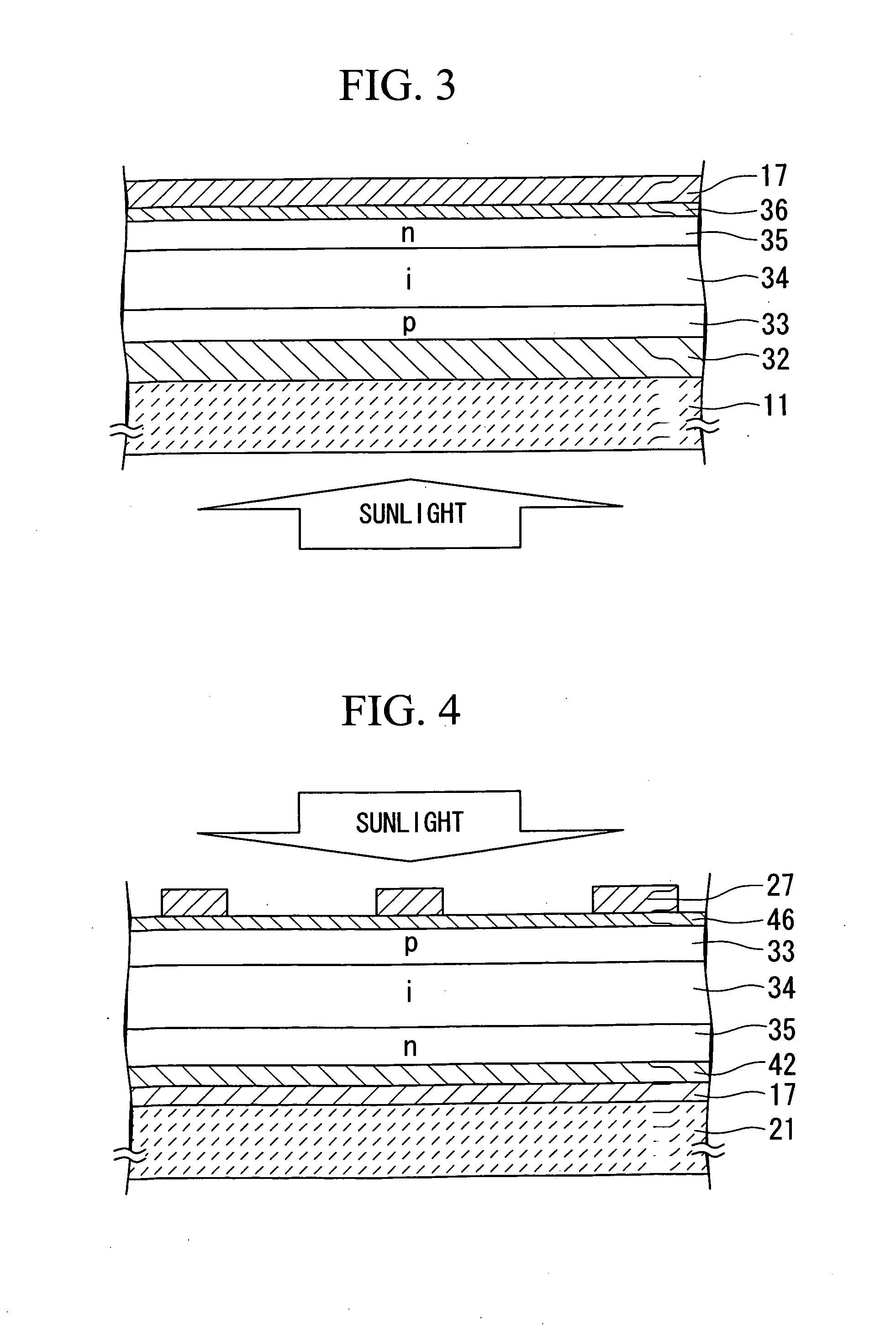
[0101] A photovoltaic device according to a third embodiment of the present invention is described with reference to FIG. 3.
[0102] Unlike the photovoltaic devices according to the first and second embodiments, the photovoltaic device according to the third embodiment has electricity-generating layers made of amorphous silicon. The photovoltaic device according to the third embodiment receives incident light via an electrically insulating transparent substrate in the same manner as with the first embodiment.
First Step
[0103] A first transparent electrode 32 is formed on an electrically insulating transparent substrate 11. Optically transparent white crown glass, for example, can be used for the electrically insulating transparent substrate 11.
[0104] The first transparent electrode 32 is made of tin oxide (SnO2).
[0105] The electrically insulating transparent substrate 11 is housed in an atmospheric plasma enhanced CVD apparatus, and the first transparent electrode 32 made of SnO2...
PUM
 Abstract
Description
Claims
Application Information