Efficient and accurate method for real-time prediction of the self-bias voltage of a wafer and feedback control of esc voltage in plasma processing chamber

a technology of self-bias voltage and plasma processing chamber, which is applied in the field of plasma etching, can solve the problems of insufficient clamping voltage to allow the wafer, risk of damaging the circuit features formed on the wafer surface, and current passing through the wafer

Active Publication Date: 2010-06-03
APPLIED MATERIALS INC
View PDF1 Cites 47 Cited by
  • Summary
  • Abstract
  • Description
  • Claims
  • Application Information

AI Technical Summary

Problems solved by technology

An insufficient clamping voltage would allow the wafer to pop off of the ESC.
An excessive clamping voltage would increase the current through the wafer to a level that risks damaging the circuit features formed on the wafer surfac

Method used


Image

  • Efficient and accurate method for real-time prediction of the self-bias voltage of a wafer and feedback control of esc voltage in plasma processing chamber
  • Efficient and accurate method for real-time prediction of the self-bias voltage of a wafer and feedback control of esc voltage in plasma processing chamber
  • Efficient and accurate method for real-time prediction of the self-bias voltage of a wafer and feedback control of esc voltage in plasma processing chamber

Examples


Embodiment Construction

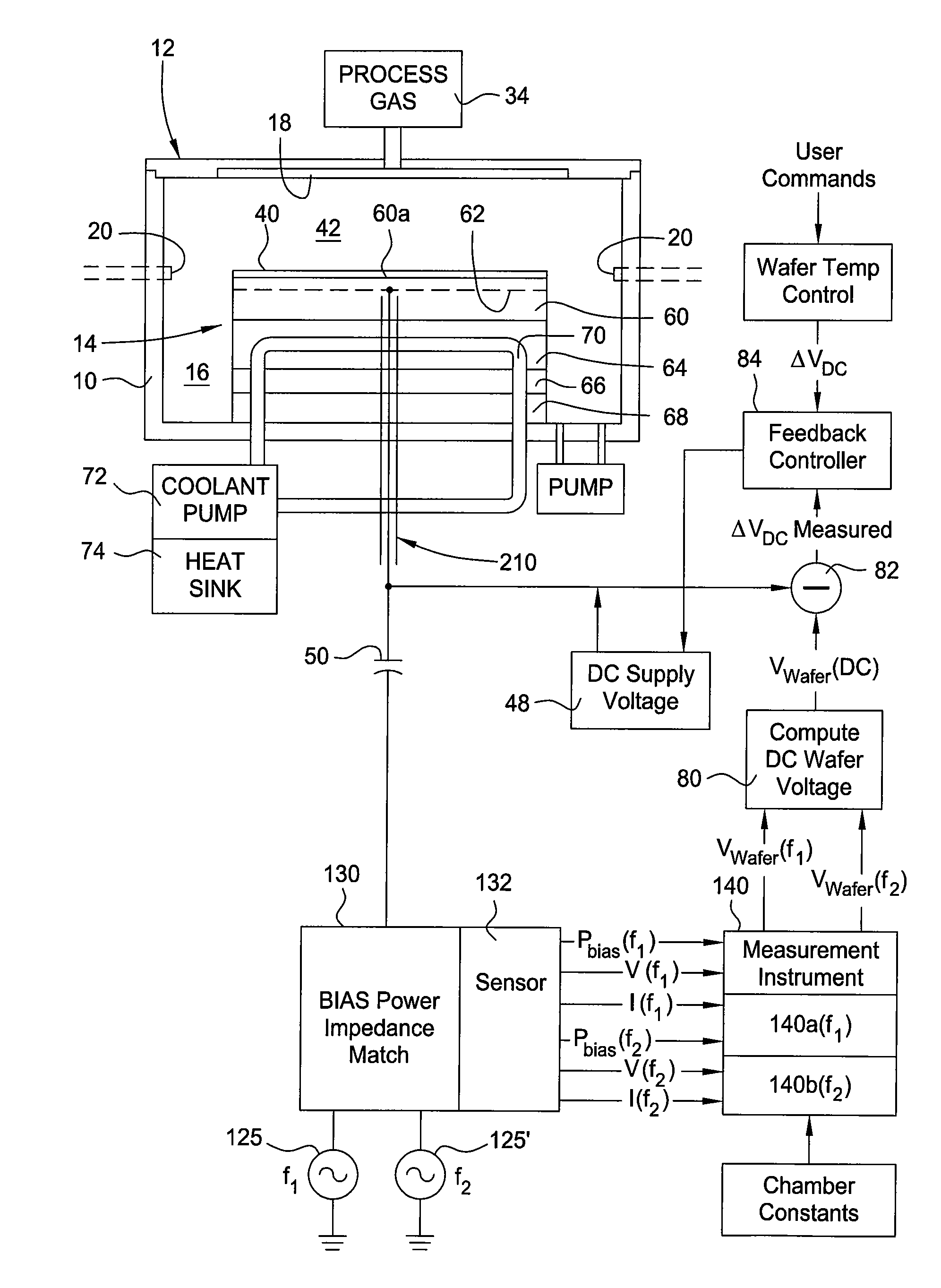
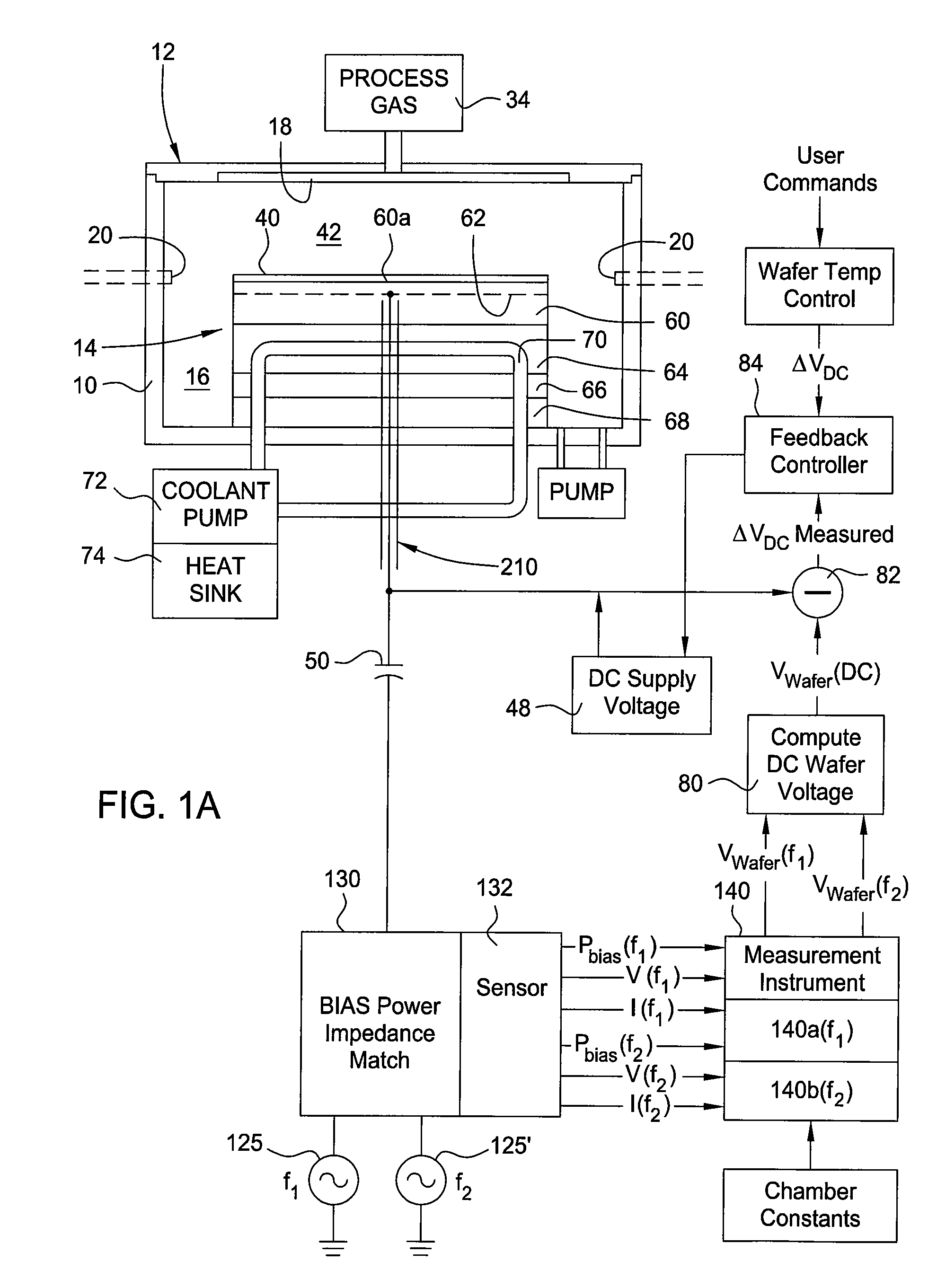
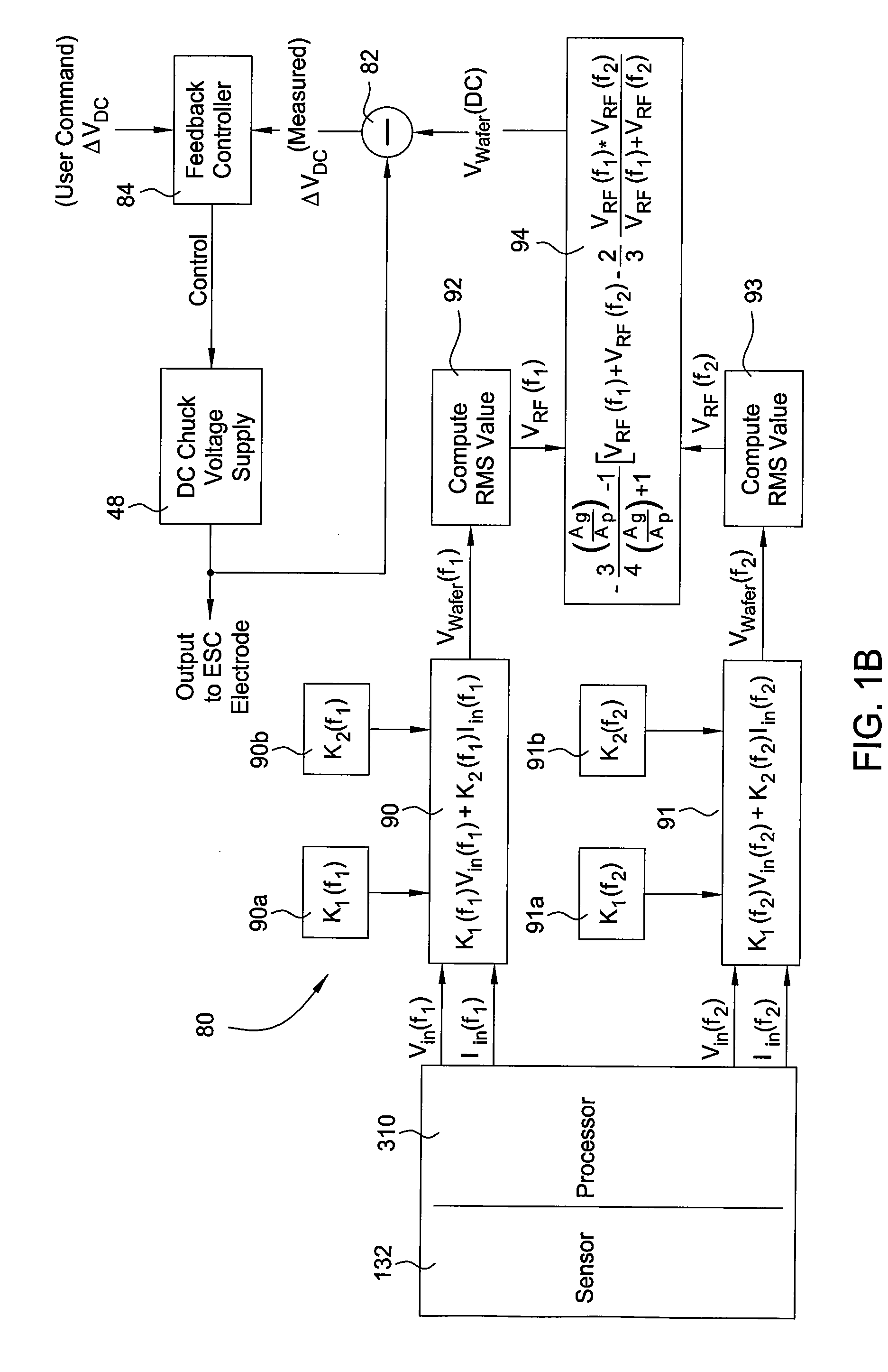
[0023]Embodiments discussed herein may provide an apparatus and method for predicting the self-bias voltage of a wafer and controlling, in real-time, at least one D.C. supply voltage source such that a clamping voltage between the wafer and the ESC is maintained.

ESC with High Contact Force Wafer Cooling

[0024]FIG. 1A illustrates a plasma reactor having a cylindrical side wall 10, a ceiling 12 and a wafer contact-cooling ESC 14. A pumping annulus 16 is defined between the ESC 14 and the sidewall 10. While a wafer contact-cooling ESC 14 may be used in any type of plasma reactor or other reactor such as thermal process reactor, the reactor in the example of FIG. 1A is of the type in which process gases can be introduced through a gas distribution plate 18 or “showerhead” forming a large portion of the ceiling 12. Alternatively, the reactor could have gas distribution inlets 20 (dashed lines) that are separate from the ceiling 12. The wafer contact-cooling ESC 14 may be employed in conju...


PUM

PropertyMeasurementUnit
Poweraaaaaaaaaa
Electric potential / voltageaaaaaaaaaa

Abstract

In a plasma reactor having an electrostatic chuck, wafer voltage may be determined from RF measurements at the bias input using previously determined constants based upon transmission line properties of the bias input, and this wafer voltage may be used to accurately control the DC wafer clamping voltage.

Description

CROSS-REFERENCE TO RELATED APPLICATION[0001]This application claims benefit of U.S. Provisional Application Ser. No. 61 / 116,883 filed Nov. 21, 2008 (Attorney Docket No. APPM / 13671L), which is incorporated by reference in its entirety.BACKGROUND[0002]1. Field[0003]Embodiments disclosed herein generally relate to plasma etching.[0004]2. Description of Related Art[0005]A plasma reactor for processing a semiconductor wafer typically holds the wafer inside the reactor chamber using an electrostatic chuck (ESC). Plasma ion energy at the wafer surface is controlled by applying a bias voltage to the wafer through the ESC. The ESC essentially consists of an insulator layer having a top surface for supporting the wafer. An electrode or conductive mesh inside the insulator layer beneath the wafer receives a D.C. voltage, creating a voltage drop across the insulator layer between the electrode and the wafer. The voltage drop produces an electrostatic force clamping the wafer to the ESC. The cla...

Claims


Application Information

Patent Timeline
IPC IPC(8): H01L21/3065
CPCH01J37/32082H01L21/6833H01J37/3299H01J37/32165
Inventor CHEN, ZHIGANGRAUF, SHAHIDMERRY, WALTER R.DORF, LEONIDRAMASWAMY, KARTIKCOLLINS, KENNETH S.
Owner APPLIED MATERIALS INC
Why Eureka
Try Eureka