Multilayer inductor

a multi-layer inductor and inductance technology, applied in the direction of inductances, magnets, magnetic bodies, etc., can solve the problems of difficult and expensive, difficult and costly, and less competitive final products, so as to improve the appreciation of the contribution of the art

Active Publication Date: 2010-06-10
ALPHA & OMEGA SEMICON INC
View PDF6 Cites 29 Cited by
  • Summary
  • Abstract
  • Description
  • Claims
  • Application Information

AI Technical Summary

Benefits of technology

[0018]There has been outlined, rather broadly, the more important features of the invention in order that the detailed description thereof that follows may be better understood, and in order that the present contribution to the art may be better appreciated. There are, of course, additional features of the invention that will be described below and which will form the subject matter of the claims appended herein.

Problems solved by technology

The disclosed power converter suffers the disadvantage that plating the deep through hole is difficult and expensive.
Although it is possible to surface mount a flip chip on top of the inductors disclosed by the above U.S. Pat. No. 6,930,584 and U.S. Published Patent Application No. 2006 / 0227518, the deposition of conductive layers, for example Cu / Ni layers on top, bottom and side walls of the inductor requires special thick metal deposition technology which is difficult and costly and makes the final product less competitive.

Method used


Image

  • Multilayer inductor
  • Multilayer inductor
  • Multilayer inductor

Examples


first embodiment

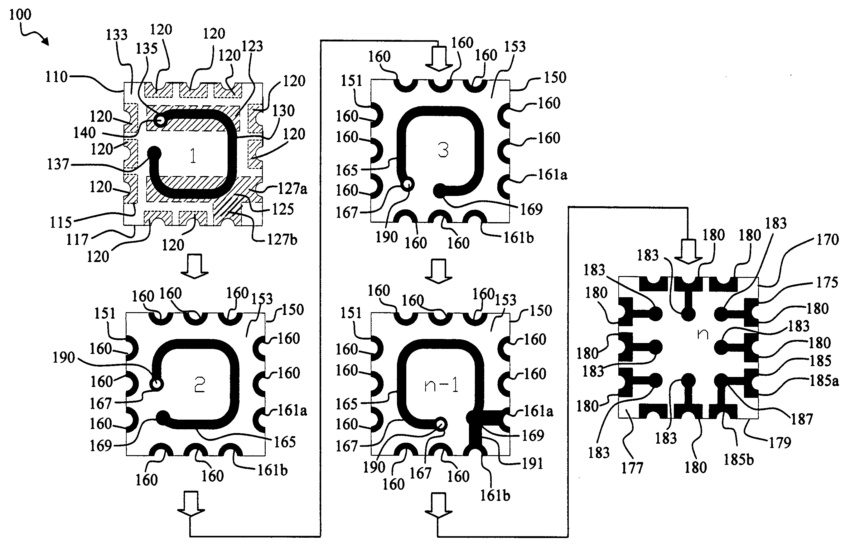
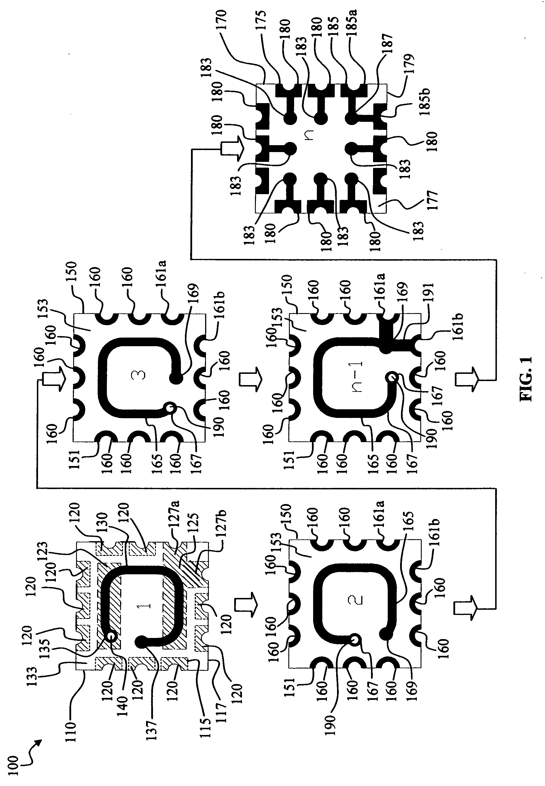
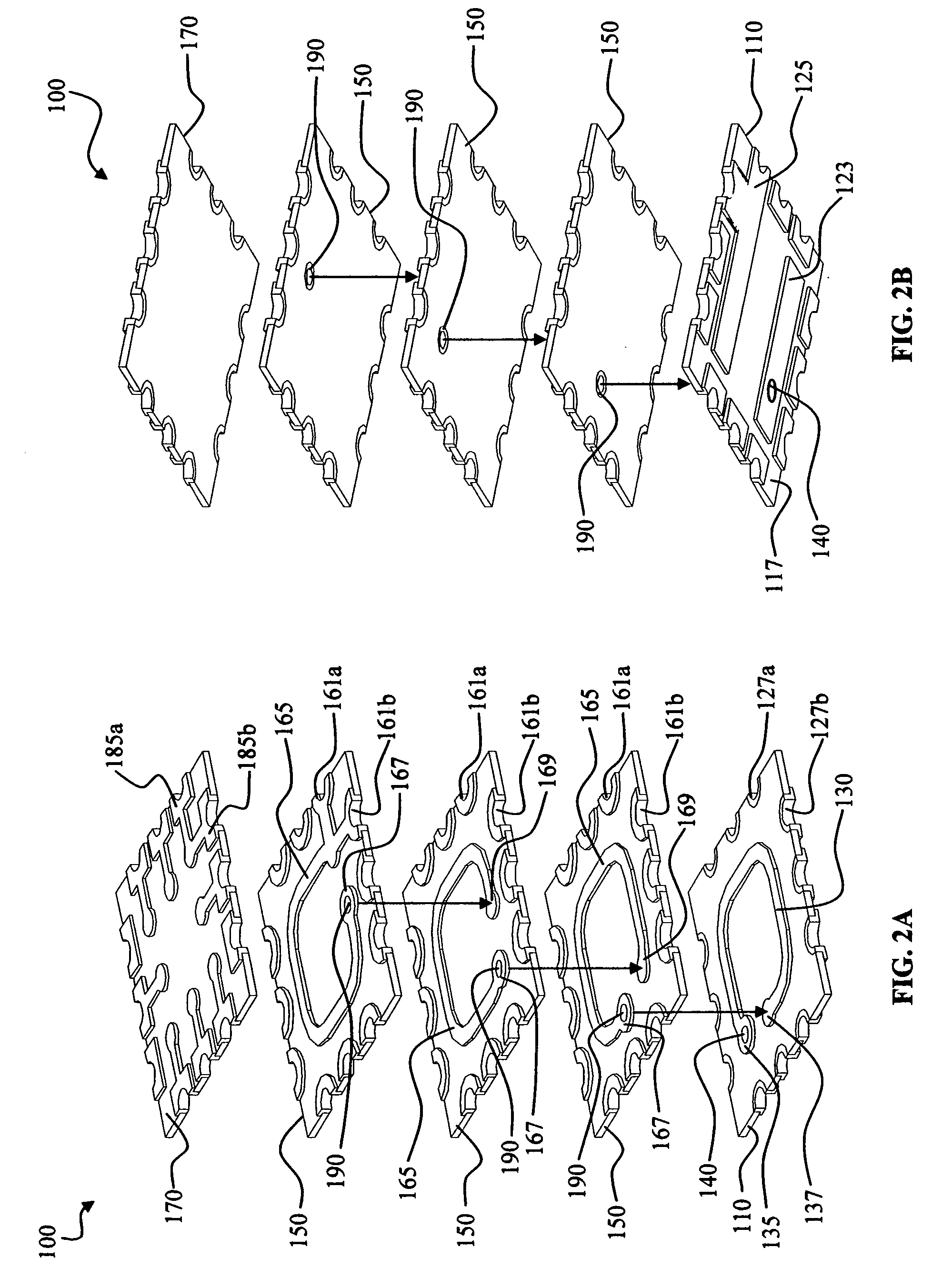
[0035]a multilayer inductor in accordance with the invention generally designated 100 is shown in FIG. 1. The multilayer inductor 100 includes a plurality n of magnetic layers laminated together including a bottom magnetic layer 110 (corresponding to layer 1), a top magnetic layer 170 (corresponding to layer n), and intermediate magnetic layers 150 (corresponding to layers 2 through n-1). The bottom magnetic layer 110 includes a bottom external conductive pattern 115 (shown in phantom lines and having a cross-hatch fill pattern) formed on a bottom surface 117 thereof. The bottom external conductive pattern 115 has a plurality of signal / power contacts 120 formed at the edges thereof. Three such signal / power contacts 120 are disposed on each of first and second adjacent sides of the bottom magnetic layer 110 in spaced relationship one to the other. Two signal / power contacts 120 are disposed on each of third and fourth adjacent sides of the bottom magnetic layer 110 in spaced relations...

second embodiment

[0052]a multilayer inductor in accordance with the invention generally designated 800 is shown in FIG. 8. The multilayer inductor 800 includes a plurality n of magnetic layers laminated together including a bottom magnetic layer 810 (corresponding to layer 1), a top magnetic layer 870 (corresponding to layer n), and intermediate magnetic layers 850 (corresponding to layers 2 through n-1). In contrast to the bottom magnetic layer 110 of the multilayer inductor 100, the bottom magnetic layer 810 does not have an inductor conductive pattern formed on a top surface 833 thereof. This may simplify the manufacturing process since only one side of the bottom magnetic layer 810 needs to have a conductive pattern formed thereon.

[0053]The bottom magnetic layer 810 includes a bottom external conductive pattern 815 (shown in phantom lines and having a cross-hatch fill pattern) formed on a bottom surface 817 thereof. The bottom external conductive pattern 815 has a plurality of signal / power conta...


PUM

PropertyMeasurementUnit
thicknessaaaaaaaaaa
conductiveaaaaaaaaaa
flux densityaaaaaaaaaa

Abstract

A multilayer inductor is disclosed. The multilayer inductor includes a bottom magnetic layer having an external conductive pattern formed on a bottom surface thereof for connection to a substrate such as a printed circuit board. The bottom external conductive pattern includes signal/power contacts and first and second inductor electrodes. A top magnetic layer includes a top external conductive pattern having signal/power contacts and inductor electrode contacts. An inductor conductive pattern formed on the top surfaces of intermediate magnetic layers disposed between the top and bottom magnetic layers are electrically coupled to each other by means of through holes to form a spiral inductor element. The spiral inductor element is coupled to the first inductor electrode by means of a through hole formed in the bottom magnetic layer and to the second inductor electrode by means of power conductive traces formed on side surfaces of the multilayer inductor. Flux density reducing layers may be inserted directly above the bottom magnetic layer and directly below the top magnetic layer. Signal/power conductive traces formed on side surfaces of the multilayer inductor provide signal/power routing between the top magnetic layer signal/power contacts and the bottom magnetic layer signal/power contacts. The top external conductive pattern accommodates a semiconductor chip in a flip chip configuration.

Description

BACKGROUND OF THE INVENTION[0001]1. Field of the Invention[0002]The present invention generally relates to multilayer inductors and more particularly to a multilayer inductor adapted to accommodate a flip chip on a top surface thereof and having conductive patterns formed on its top, bottom and side surfaces.[0003]2. Description of Related Art[0004]Multilayer inductors are well known in the art. For example a chip-type inductor comprising a laminated structure is disclosed in U.S. Pat. No. 4,543,553. The structure includes a plurality of magnetic layers in which linear conductive patterns extending between the respective magnetic layers are connected successively in a form similar to a coil so as to produce an inductance component. The conductive patterns formed on the upper surfaces of the magnetic layers and the conductive patterns formed on the lower surfaces of the magnetic layers are connected with each other in the interfaces of the magnetic layers and are also connected to ea...

Claims


Application Information

Patent Timeline
Patent Type & Authority Applications(United States)
IPC IPC(8): H01F5/00H01F41/04
CPCH01F17/0013H01F27/29Y10T29/4902Y10T29/49069Y10T29/49073H01F41/046H01L2224/16235H01L2924/15311H01L2924/13091H01L2924/00
Inventor LU, JUNHEBERT, FRANQOIS
Owner ALPHA & OMEGA SEMICON INC
Why Eureka
Try Eureka