
Semiconductor device storage cell structure, method of operation, and method of manufacture

a technology of semiconductor integrated circuit devices and storage cells, which is applied in the direction of digital storage, semiconductor devices, instruments, etc., can solve the problems of complex manufacturing process of capacitor structures and the need to refresh data values

Inactive Publication Date: 2010-06-17
SUVOLTA
View PDF1 Cites 101 Cited by
  • Summary
  • Abstract
  • Description
  • Claims
  • Application Information

AI Technical Summary

Benefits of technology

The solution results in a storage cell that retains charge longer than conventional DRAM cells, reducing the frequency of refresh operations, enhancing performance, and lowering power consumption while simplifying manufacturing by eliminating the need for capacitor contact locations.

Problems solved by technology

A drawback to such arrangements can be the complexity involved in manufacturing the capacitor structures.
However, because charge can leak from a DRAM capacitor, such cells require a periodic “refresh”.
This is one drawback to DRAM memories, the need to refresh data values periodically in order to ensure data values are not lost.

Method used


Image

  • Semiconductor device storage cell structure, method of operation, and method of manufacture
  • Semiconductor device storage cell structure, method of operation, and method of manufacture
  • Semiconductor device storage cell structure, method of operation, and method of manufacture

Examples


first embodiment

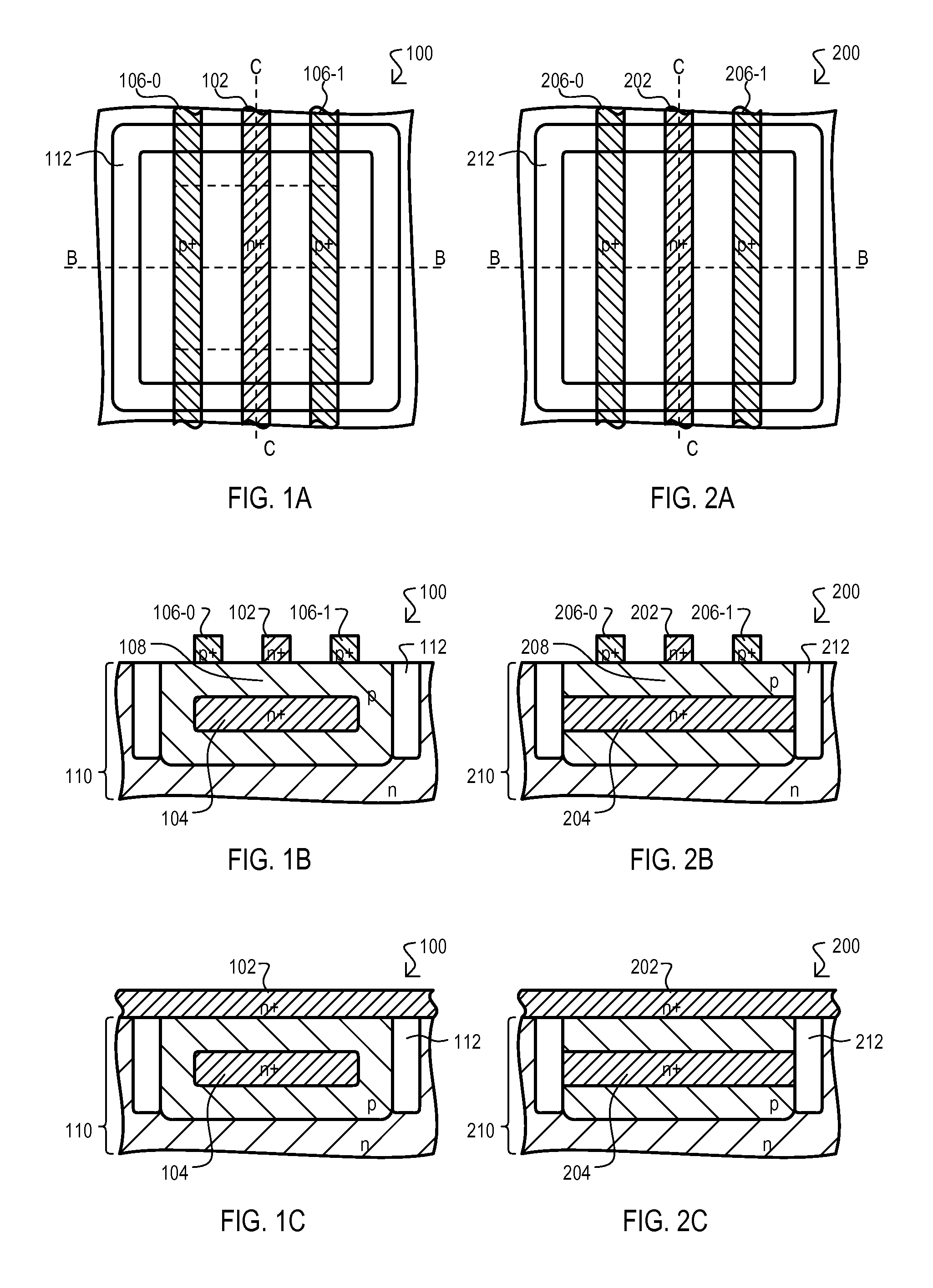
[0049]Referring now to FIGS. 1A to 1C, a storage cell is shown in a series of views, and designated by the general reference character 100. FIG. 1A is a top plan view of storage cell 100. FIG. 1B is a side cross sectional view taken along line B-B of FIG. 1A. FIG. 1C is a side cross sectional view taken along line C-C of FIG. 1A.

[0050]As shown in the various views, a storage cell 100 can include a control gate 102, a store gate 104, a first source / drain 106-0, a second source / drain 106-1, and a channel region 108. A storage cell 100 can be formed in a substrate 110, and can be bounded by an isolation structure 112.

[0051]A control gate 102 can be patterned from a semiconductor layer formed on a surface of a substrate 110, and can be doped to one conductivity type (in this example, n-type). In the particular example shown, control gate 102 can extend over, and be in physical contact with channel region 108 between opposing ends of isolation structure 112.

[0052]A store gate 104 can be...

second embodiment

[0060]Referring now to FIGS. 2A to 2C, a storage cell is shown in a series of views, and designated by the general reference character 200. FIGS. 2A to 2C show the same general views as FIGS. 1A to 1C. Further, a storage cell 200 can include some of the same general structures as storage cell 100. Accordingly, like structures will be referred to by the same reference character but with the first digit being a “2” instead of a “1”.

[0061]Storage cell 200 can differ from that of FIGS. 1A to 1C in that a store gate 204 is not completely surrounded by oppositely doped semiconductor material, and can abut isolation structure 212. Such an arrangement can result in greater charge leakage than the embodiment of FIGS. 1A to 1C, but may still provide for slower refresh rates than conventional DRAMs. In addition, a storage cell 200 may be more easily manufactured, by requiring fewer masks, or may provide more uniform performance as a storage gate position 204 may vary less according to mask al...

third embodiment

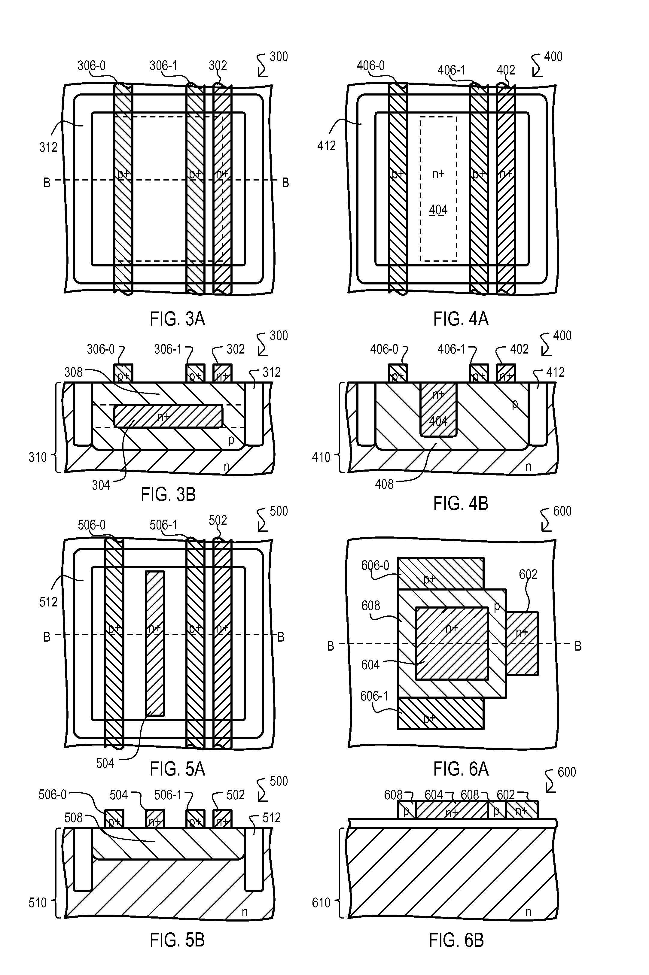
[0063]Referring now to FIGS. 3A and 3B, a storage cell is shown in a series of views, and designated by the general reference character 300. FIGS. 3A and 3B show the same general views as FIGS. 1A and 1B. Further, a storage cell 300 can include some of the same general structures as storage cell 100. Accordingly, like structures will be referred to by the same reference character but with the first digit being a “3” instead of a “1”.

[0064]Storage cell 300 can differ from that of FIGS. 1A to 1C, in that a position of control gate 304 can be different. In the case of FIGS. 1A to 1C, a control gate 104 is situated between first and second source / drains (106-0 and 106-1) in a direction parallel to a surface of substrate 110 (considered herein the lateral direction). In the arrangement of FIGS. 3A and 3B, a control gate 304 is not situated between source / drains (306-0 and 306-1), but rather to one side of both such structures in the lateral direction.

[0065]In an arrangement like that of...


PUM


Abstract

A method of fabricating an integrated circuit device storage cell may include forming a channel region comprising a semiconductor material doped to a first conductivity type; forming a store gate structure comprising a semiconductor material doped to a second conductivity type in contact with the channel region; and forming a control gate terminal from at least a portion of a semiconductor layer deposited on a substrate surface in contact with the channel region, the portion of the semiconductor layer being doped to the second conductivity type.

Description

[0001]This application is a divisional of U.S. patent application Ser. No. 11 / 799,572 filed on May 1, 2007, the contents of which are incorporated by reference herein.TECHNICAL FIELD[0002]The present invention relates generally to electronic storage devices, and more particularly to storage cells for storing data in a semiconductor integrated circuit device.BACKGROUND OF THE INVENTION[0003]An important feature of many integrated circuit (IC) devices can be the ability to store a data value. Numerous examples of conventional storage devices are known, including nonvolatile storage devices and volatile storage devices. Volatile storage devices can include static random access memories (SRAMs) as well as dynamic RAMs (DRAMs). DRAMs are often preferred in many applications due to their lower power consumption and smaller cell size.[0004]A typical conventional DRAM cell includes a metal-oxide-semiconductor (MOS) pass transistor and a storage capacitor. A DRAM capacitor can have many conf...

Claims


Application Information

Patent Timeline
Patent Type & Authority Applications(United States)
IPC IPC(8): G11C11/24H01L27/108G11C11/34H01L21/8242H10B12/00
CPCG11C11/404H01L27/098H01L27/108H01L29/808H01L29/1066H01L29/42316H01L29/66901H01L29/1058H10B12/00
Inventor VORA, MADHU B.
Owner SUVOLTA
Learn More