

Solid-state imaging device and manufacturing method of the same, electronic equipment, and semiconductor device
a manufacturing method and solid-state imaging technology, applied in the direction of radiation controlled devices, semiconductor/solid-state device details, optical radiation measurement, etc., can solve the problems of reducing sensitivity but also color mixing and lower resolution, affecting the adhesion of other materials, and affecting the image quality and yield of the same, so as to reduce the deterioration of image quality and yield due to the crack, the effect of reducing the deterioration of image quality and yield
Active Publication Date: 2010-06-24
SONY CORP
View PDF6 Cites 34 Cited by
- Summary
- Abstract
- Description
- Claims
- Application Information
AI Technical Summary
Benefits of technology
[0027]In the solid-state imaging device according to the embodiment of the invention, the interface between the first light transmission layer and the second light transmission layer is formed in contact with the guard ring, and therefore, even when a crack occurs, the crack stops at the guard ring, and deterioration in image quality and yield due to the crack can be reduced.
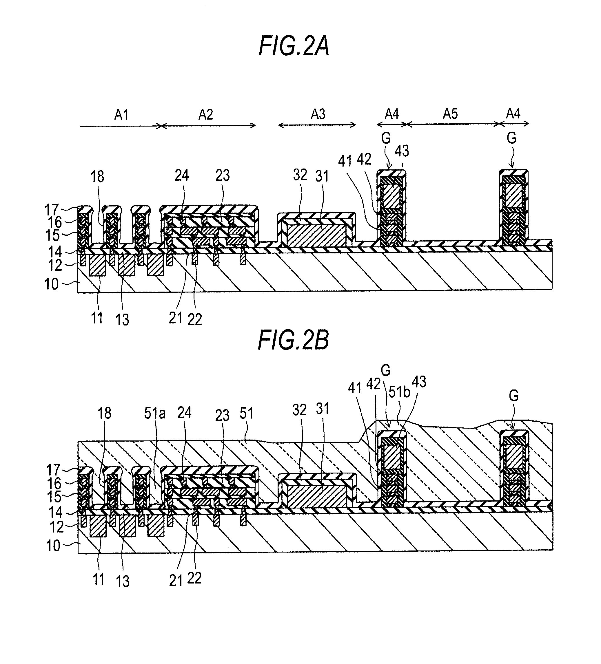
[0028]Further, in the solid-state imaging device of the embodiment according to the invention, the first light transmission layer is removed at least in a part of the dicing area, and no crack due to the first light transmission layer occurs at dicing and deterioration in image quality and yield due to the crack can be reduced.
[0029]In the manufacturing method according to a solid-state imaging device of the embodiment of the invention, the interface between the first light transmission layer and the second light transmission layer is formed in contact with the guard ring, and therefore, even when a crack occurs, the crack stops at the guard ring, and deterioration in image quality and yield due to the crack can be reduced.
[0030]Further, in the manufacturing method of a solid-state imaging device according to the embodiment of the invention, the first light transmission layer is removed at least in a part of the dicing area, and no crack due to the first light transmission layer occurs at dicing and deterioration in image quality and yield due to the crack can be reduced.
[0031]The electronic equipment according to the embodiment of the invention, in a solid-state imaging device forming the electronic equipment, deterioration in image quality and yield due to the crack can be reduced.
[0032]The semiconductor device according to the embodiment of the invention, in a semiconductor device having a layer of a siloxane resin, deterioration in image quality and yield due to the crack can be reduced.
Problems solved by technology
However, if the area per unit pixel is reduced, the amount of light entering the photodiode forming the photoelectric conversion part is not sufficient.
Accordingly, light entering obliquely does not reach the photodiode region but enters an adjacent photodiode, and not only reduction in sensitivity but also color mixing and lower resolution are caused.
Generally, the outer side of siloxane is covered by methyl groups having non-polarity and the like and shows water / oil repellency, and has poor adhesion to other materials.
Further, when the siloxane film is heated and hardened for three-dimensional cross-linkage to increase its strength, the siloxane film becomes brittle.
The siloxane in which inorganic nanoparticles are put for raising the refractive index is especially brittle, and a crack easily occurs.
The siloxane film has low adhesion to the upper and lower films as described above, and is brittle and the crack easily progresses.
Starting from the crack C, peeling easily occurs at the interface between the siloxane film and the upper film and the interface between the siloxane film and the lower film in poor adhesion.
If the peeling of the films progresses from the scribing part to the pixel part, image quality becomes deteriorated.
Further, when chippings produced by dicing are attached onto the on-chip lenses in the pixel area, light does not reach the photodiodes in the part with the chippings thereon and the output signal level becomes lower, and these lead to deterioration in image quality.
When the siloxane resin is used as the material of the core part of the optical waveguide as described above, peeling occurs at the interface between the siloxane and the upper layer or the lower layer during dicing and reaches the pixel area, chippings produced by dicing are attached to the pixel area, and thereby, deterioration in image quality and yield is caused.
Method used
View moreImage
Smart ImageViewing Examples

Examples
first embodiment (
1. First Embodiment (Configuration in which interface between first light transmission layer and second light transmission layer is contact with guard ring)
second embodiment (
2. Second Embodiment (Configuration in which first light transmission layer is removed in part of dicing area and second light transmission layer is formed in removed part)
third embodiment (
3. Third Embodiment (Configuration in which first light transmission layer and second light transmission layer are removed in part of dicing area)
Login to View More PUM
| Property | Measurement | Unit |
|---|---|---|
| refractive index | aaaaa | aaaaa |
| refractive indices | aaaaa | aaaaa |
| thickness | aaaaa | aaaaa |
Abstract
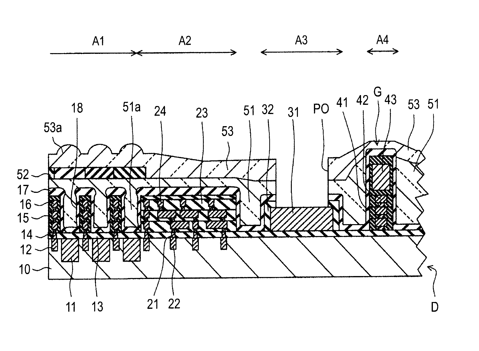
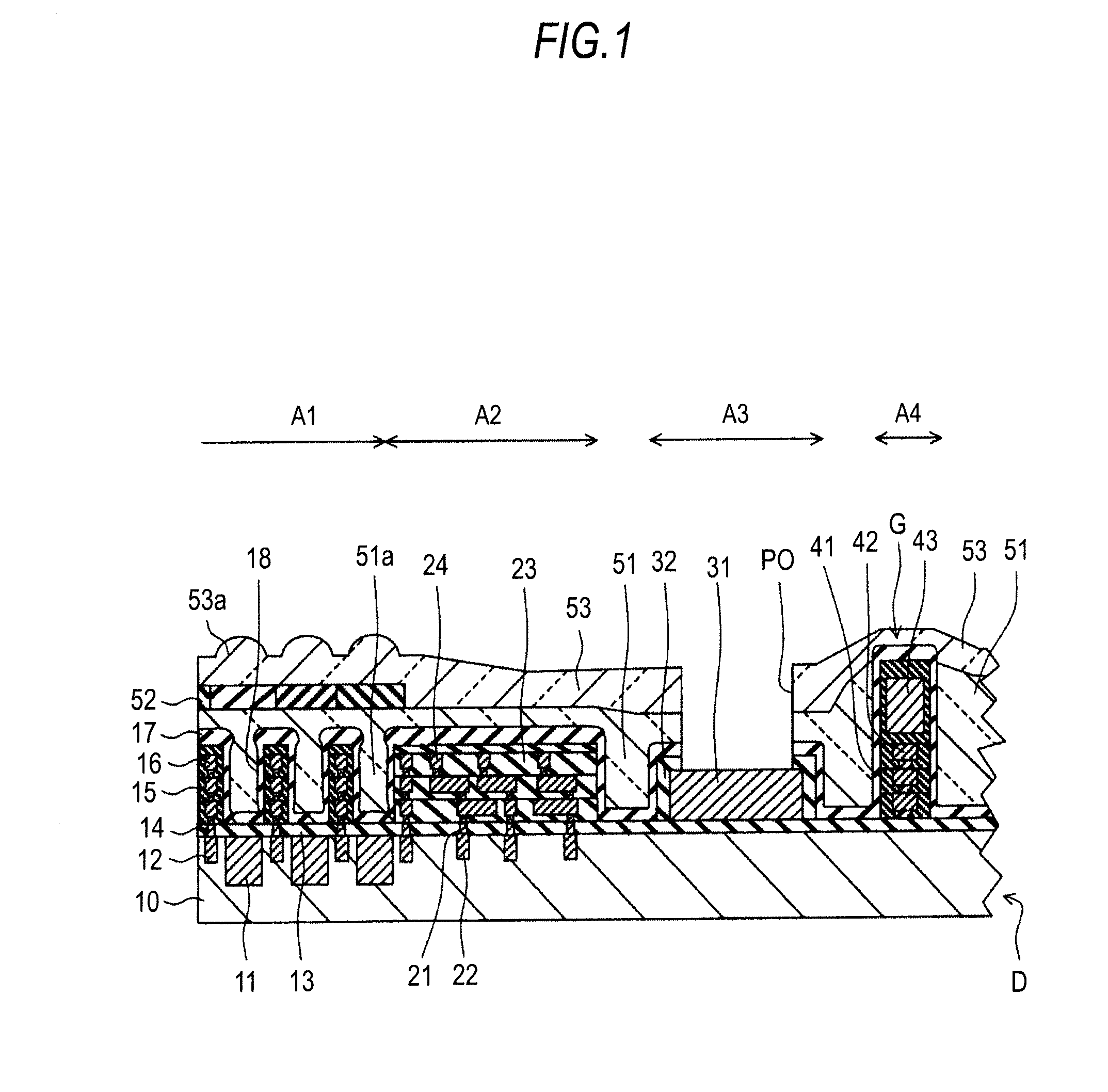
A solid-state imaging device includes: a photodiode formed to be segmented with respect to each pixel in a pixel area in which plural pixels are integrated on a light receiving surface of a semiconductor substrate; an insulator film formed on the semiconductor substrate to cover the photodiode; a recessed part formed with respect to each of the pixels in the insulator film in an upper part of the photodiode; a first light transmission layer of a siloxane resin formed to fill the recessed part and configure an optical waveguide in the pixel area; a second light transmission layer formed to configure an on-chip lens with respect to each of the pixels in the pixel area; and a guard ring formed to surround an outer circumference of the pixel area to partition an inner area containing the pixel area and an outer dicing area.
Description
[0001]The present application claims priority to Japanese Patent Application JP 2008-314510 filed in the Japanese Patent Office on Dec. 10, 2008, the entire contents of which is hereby incorporated by reference.BACKGROUND OF THE INVENTION[0002]1. Field of the Invention[0003]The present invention relates to a solid-state imaging device and a manufacturing method of the same, electronic equipment, and a semiconductor device, and specifically, to a solid-state imaging device in which pixels having photodiodes are arranged in a matrix on a light receiving surface and a manufacturing method of the same, electronic equipment including the solid-state imaging device, and a semiconductor device.[0004]2. Background Art[0005]In a solid-state imaging element represented by a CCD and a CMOS image sensor used for an area sensor, a photoelectric conversion part of photodiodes, a wiring part that transmits generated signals, transistors, etc. are formed on a semiconductor substrate. The element ha...
Claims
Login to View More Application Information
Patent Timeline
 Patent Type & AuthorityApplications(United States)
IPC IPC(8): G01J1/04H01L31/0232H01L31/18H01L23/00H01L21/301H01L27/14H01L27/146H04N25/00
CPCH01L27/14636H01L2224/05Y10S148/07H01L27/14618H01L27/14621H01L27/14625H01L27/14627H01L27/14632H01L27/14645H01L29/0619H01L29/0623
InventorHIRANO, HIDEKIOGINO, AKIKONISHIKIDO, KENJUSUGIURA, IWAOAJISAWA, HARUHIKOYOSHIHARA, IKUO
OwnerSONY CORP